The death of copper as a signal transmission medium has erroneously been forecasted for decades, Nevertheless, consensus is building that the technology’s obituary will soon be published for at least one application in the near future. End-of-life for copper as a vehicle for high-speed silicon input/output (I/O) should occur around the time 51.2-Tbps switch chips hit the market, many agree. Facebook and Microsoft are among these doomsayers, which led the two data center giants to form the Co-Packaged Optics Collaboration in March 2019. The organization seeks to drive technology developers towards the integration of optical communications capabilities with switch chips and other silicon devices to carry on when copper’s capabilities expire.
Members of the collaboration, via an effort through the Joint Development Foundation, helpfully issued a document this past February that models what data center network operators such as Facebook and Microsoft would like to see. Of course, having a destination is one thing; figuring out how you’re going to get there is another. While organizations such as OIF and the Consortium for On-Board Optics (COBO) have launched projects to drive consensus and standardization of approaches, several technical challenges – including “module” design, placement of the light source, and connectivity – promise to challenge the ingenuity of the technology supply chain.
Two Paths toward the Same Destination
This past February’s 28-page “3.2 Tb/s Copackaged Optics Optical Module Product Requirement Document” (PRD) offers what should prove to be useful guidelines for co-packaged optics development. The PRD spells out desired transmission modes – 200GBASE-FR4 and 400GBASE-FR and -DR – as well as such other design elements as electrical specifications, optical and electrical connectors, mechanical characteristics, management interfaces, and related elements.
The PRD envisions the module will include a digital signal processor (DSP), modulator driver and TIA chips, and an optical transmitter and receiver combination based on silicon photonics regardless of operating mode. The 400GBASE-FR4 variant also will feature optical multiplexer and de-multiplexer capabilities as well as support of up to 3-km reaches on duplex single-mode fiber. This version also must be capable of operating in 200BASE-FR4 mode – apparently for lower-speed requirements rather than providing a road to 3.2 Tbps via a greater number of optical and electrical channels. Speaking of electrical channels, the PRD calls for the transceiver electrical interface to be based on 32×106G electrical lanes in compliance with CEI-112G-XSR. The electrical interface rates will drop to 32×53G PAM4 when in 200BASE-FR4 operation.
The collaboration, undoubtedly based on input from the technology development community, cited two approaches in the PRD when it comes to the positioning of the laser: internal and external. The two alternatives have arisen as researchers ponder the challenges posed by putting a cooled laser next to a very hot running switch chip.
The internal approach – where the laser is part of the co-packaged optical module – certainly would appear the more elegant and efficient. However, as the laser represents the module component most likely to fail, particularly in the thermal environment in which it will operate, reliability remains a concern among potential network operators. The PRD calls for a backup laser in such configurations, for example.
Nevertheless, several parties are pursuing the internal option. “For the co-packaged approach, our view has been for quite a while that the only way to make that work is with silicon photonics. And so you have silicon photonics that is very compact that you put right next to the switch ASIC or other IC that you want to co-package it with on the same substrate,” commented Robert Blum, senior director of new business for Intel’s Silicon Photonics Product Division, during May’s Lightwave and Broadband Technology Report High Speed Networking 2.0 virtual conference. “Now, at Intel we have what we call this hybrid laser where we can integrate gain on the chip on the silicon photonics and make the lasers on the same chip…So we have it all as part of the same co-packaged ASIC chip.”
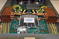
Assuming the thermal challenges can be met – “We’re very comfortable with the thermal solutions we’re working on,” Blum stated – the internal approach is relatively straightforward. The company prepped a demonstration for last year’s OFC that showed a 1.2-Tbps co-packaged optics implementation using such modules (Figure 1).
But not everyone who wants to play in the space has internal laser technology – or perhaps believes such an approach can meet the thermal performance and reliability requirements. Thus there are multiple companies working with external laser sources. One is Ayar Labs, which is developing “chiplets” that integrate all of the transceiver functions save the laser source, which can be housed outside of the switch and be used to feed multiple chiplets. The company is developing an external laser as well. Meanwhile, IBM Inc., Ranovus, TE Connectivity, and Senko Advanced Components, Inc. have unveiled a co-packaged optics partnership focused on the use of the Ranovus Odin 32 silicon photonics engine based on multi-wavelength quantum dot laser (QDL) and micro ring resonator technologies.
Removing the laser from the co-packaged optics assemblies should make them smaller, obviate the thermal challenges, and make it possible to overcome laser failure without having to replace the board or design in a backup light source. However, the approach brings issues of its own. Foremost among these is getting the light to the chiplets, which sources agree will require the use of polarization maintaining fiber. Accommodating such fibers and the optical power they will have to carry only adds to connectivity issues co-packaged optics faces.
Getting Connected
At the May Lightwave and Broadband Technology Report online conference, Tom Mitcheltree, applications engineering manager at connectivity company US Conec, described an experiment Corning performed to determine how end-face and connector cleanliness affected the amount of optical power a connected fiber could support. A fiber with a pristine end-face/connector pairing could handle a full Watt of optical power, which should be sufficient for several co-packaged optics applications. However, add contaminants to the end face and the power-handling capabilities dropped significantly while threatening damage to the connector from excess heat, Mitcheltree stated.
Brad Booth, principal hardware engineer for Microsoft’s Azure Hardware and Architecture Group and chairman of COBO, provided additional context during the same event. “You can’t use connectors that we think that we can use today only because, if there is any type of impairment, any type of dust or particulate that’s on that mating of that connector, you basically will burn that connector,” he said. “It’ll just explode.”
The development of connectivity options that won’t explode is one of the points of focus for COBO’s Co-Packaged Optics (CPO) Working Group, which it formed late last year. COBO’s specification work for onboard optics – which involve connecting an onboard optical module to the silicon it supports – translates well to the requirements of co-packaged optics, particularly approaches with an external laser, according to Booth. Members of COBO are working on several potential approaches to bringing fiber to the chiplets or co-packaged modules, with expanded beam connectors and non-contact connectors among the options under consideration. Well-known connector suppliers such as US Conec and Senko Advanced Components are among the companies working with these technologies, alongside emerging players such as Arrayed Fiberoptics who have positioned their non-contact connector technology for such applications.
Less exotic but perhaps only slightly less challenging is the matter of faceplate connectivity, thanks to the number of fibers co-packaged optics will require. A 51.2-Tbps switch chip will require sixteen 3.2-Tbps co-packaged optical modules to meet its needs. If the optical modules are based on 400GBASE-DR4, the implementation would require 1024 fibers, US Conec’s Mitcheltree pointed out during the online event. Even the fiber-saving use of multiplexing with FR4 would still mean 256 fibers going in and out of a box as small as 1RU. And that wouldn’t count the fibers required with external lasers, a number most agree would be at least four.
Mitcheltree stated that some sort of multifiber connector would be necessary to meet the requirements without having to expand platform size. MPO-16s might work for both FR4 and DR4 implementations but wouldn’t leave much room on the faceplate for anything else, such as connecting external lasers, particularly with DR4. A new connector type, which US Conec is calling MMC, likely will be needed, Mitcheltree stated. Such a connector also would be able to accommodate 16 fibers, if not more, in a smaller format than an MPO-16.
To handle all the different requirements that might be needed among the various co-packaged design options, Mitcheltree estimates there are at least nine technologies the connectivity community will have to supply. As shown in Figure 2, these elements are in various stages of development.
Target Dates
With switch developers already contemplating 51.2-Tbps devices, the clock is ticking on the development of co-packaged optics approaches. LightCounting, in a report published last December, forecasted that initial implementations of co-packaged optics might appear as soon as next year, perhaps to support high-performance computing applications. However, it seems clear that full technological maturity will take a few years.
“There’s a lot of complexity with CPO and it’s going to be a while,” commented Booth. "People have shown proof of concepts and you can build one-offs, but to create an ecosystem in an industry where everybody can play, that’s going to take a little while. We’re hoping by 2025 we start to see that ecosystem come into development, people building and deploying these pieces of equipment.”
Stephen Hardy is editorial director of Lightwave.

Stephen Hardy | Editorial Director and Associate Publisher, Lightwave
Stephen Hardy is editorial director and associate publisher of Lightwave and Broadband Technology Report, part of the Lighting & Technology Group at Endeavor Business Media. Stephen is responsible for establishing and executing editorial strategy across the both brands’ websites, email newsletters, events, and other information products. He has covered the fiber-optics space for more than 20 years, and communications and technology for more than 35 years. During his tenure, Lightwave has received awards from Folio: and the American Society of Business Press Editors (ASBPE) for editorial excellence. Prior to joining Lightwave in 1997, Stephen worked for Telecommunications magazine and the Journal of Electronic Defense.
Stephen has moderated panels at numerous events, including the Optica Executive Forum, ECOC, and SCTE Cable-Tec Expo. He also is program director for the Lightwave Innovation Reviews and the Diamond Technology Reviews.
He has written numerous articles in all aspects of optical communications and fiber-optic networks, including fiber to the home (FTTH), PON, optical components, DWDM, fiber cables, packet optical transport, optical transceivers, lasers, fiber optic testing, and more.
You can connect with Stephen on LinkedIn as well as Twitter.

