Erbium-doped waveguide amplifiers promote optical-networking evolution
Waveguide technology advances coincide with metro market needs for compact, high-functionality, lower-cost components.
DENIS BARBIER, Teem Photonics
With the unrelenting growth in data-communications traffic, the evolution of WDM beyond long-haul applications into metropolitan area networks (MANs), and the inability of carriers to keep pace with bandwidth demand, the call for more compact, more functional, lower-priced optical components is becoming all the more compelling. Advances in integrated optical devices based on waveguide technology present admirable opportunities to meet these challenges head-on.
Waveguide amplifiers, in particular, are new integrated optical products well suited to MAN applications. Some of the intrinsic benefits for using waveguide amplifiers in MAN applications include their compactness, reliability/performance, flexibility, and lower-cost processing.
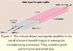
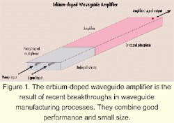
As the name implies, an erbium-doped waveguide amplifier (EDWA) consists of waveguides embedded in an amorphous erbium-doped glass substrate (see Figure 1). The erbium atoms provide the glass with gain in the 1,550-nm fiber-optic window. The waveguide itself is a localized increase in the glass refractive index. Today's manufacturers have several methods available to produce erbium-doped glass waveguides: PECVD and flame hydrolysis deposition, sputtering, ion-exchange, or ion implantation.For the manufacture of waveguide amplifiers, the two most advanced methods are ion-exchange and sputtering. The process of producing erbium-doped glass waveguides consists of two principal steps.
The first step is to prepare doped material. A glass block is prepared using standard melting techniques, with erbium being added as erbium oxide powder at an early preparation stage. Two types of oxide glasses are currently used to produce waveguide amplifiers: alumino-silicate and alumino-phosphate. The main advantage of these glasses is that they accept a very high doping level of erbium (more than 1026 atoms/m3), which is at least 100 times higher than in silica glass. During the preparation of these glasses, special care is taken to eliminate OH impurities, which would create strong nonradiative de-excitation of pumped erbium ions.1
The second step is to make the waveguide. Using the ion-exchange technique, channel waveguides are made in the oxide bulk glasses. The waveguides are then buried a few microns below the glass surface. Burying the waveguides ensures their stability and optimizes their performance. As the waveguides are no longer in contact with the substrate surface, they support confined modes with low propagation losses and low polarization dependence as well as maintain very good compatibility with optical fibers. The ion-exchanged waveguides benefit from sustaining the same spectroscopic properties as the starting material.
The other promising method for producing erbium-doped glass waveguides is the sputtering deposition technique. Currently under development by Lucent Technologies, sputtering is the process by which ions on bulk glasses are ejected under the action of ion-beam irradiation.2 The bulk glasses, used as a sputtering target, form an erbium-doped thin-glass layer on a silica wafer or on a silica-buffered silicon wafer. After an etching process, the thin film is transformed into channel waveguides. These channel waveguides can support highly confined modes with moderate propagation losses when protected by a cladding layer. The sputtered material may have different spectroscopic properties than the starting one.
Of the two processes, to date, only the ion-exchange method has matured enough to be used to manufacture waveguide products, notably passive components. Among those manufacturers, only a very few have succeeded in making active components such as erbium-doped waveguide amplifiers.
EDWAs are inherently compact. Without the need to accommodate meters upon meters of fiber and with the ability to integrate numerous functions, the slim-line elegance of EDWAs is perfectly adapted to applications in restricted-space environments. One of the smallest gain block amplifiers to date, featuring 15-dB gain at 1,535 nm, fits in a 130x11x6-mm package.
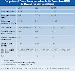
EDWAs also offer a better price/performance ratio than comparable EDFAs for access and metro network applications. For long-haul WDM transmissions where high performance is necessary, multistage EDFAs lead. However, continued EDWA development will progressively minimize the performance difference. EDWA performance figures are as follows: 15-dB gain at peak wavelength, 4.5-dB noise figure over the entire C-band, and 7-dBm output power (12 dBm when a double pump scheme is used).The EDWA has the advantage of inheriting the fundamental qualities of the EDFA, such as a low noise figure, negligible polarization dependence, and the absence of interchannel crosstalk. That's in contrast to other integrated amplifier technologies, such as the semiconductor optical amplifier (see Table).
Costs are kept in check because of integration technology. While the integration of functions is a highly complex and sophisticated procedure, the ion-exchange process is a very elegant and inexpensive way of producing key optical functions.
Most of the intrinsic advantages of EDWAs come from their ability to provide high gain in very short optical paths. This capability gives vendors more flexibility in the design of a compact amplifier.
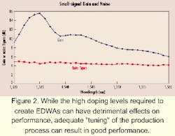
High gain in short optical paths is achieved by applying high erbium-doping levels to the glass that maximize the creation of large gain per unit length. Yet, there is a limitation: The more erbium ions added to the glass, the closer they become, which increases the likelihood of the formation of clusters. When excited, the erbium ions in the clusters start exchanging energy. When that occurs, the erbium ions reduce their efficiency.The critical turning point in the process is finding a compromise between the high erbium-doping level, which helps create large gain per unit length, and the parasitic effects of high doping levels, which hinder erbium ions from providing gain. Establishing the compromise is the key to producing a reliable and efficient integrated optical-amplifier device. Thus far, only a few laboratories and R&D departments worldwide have mastered this fine-tuning in-production technique (see Figure 2).
For an optical amplifier device to become "ready to use," it needs other optical components, such as a pump, multiplexer, filters, tap couplers, and mode adapters. The ability to integrate these functions onto a single chip provides three key benefits. The reliability of the chip increases since integration eliminates the need to splice components, and the throughput increases because fewer production steps are required.
One downside to this integration procedure is that for maximum amplifier performance, functions other than amplification must be made on undoped material. This situation is remedied by employing the monolithic integration of doped and undoped waveguides, which provide added advantages. This technique provides additional reliability and greatly reduces the potential failure rate brought about by soldering or the gluing of pieces together.
For OEM customers, the major benefit of integration is that EDWAs can be easily built into their own products.
EDWAs also can be combined in a very compact way with any lossy components, such as splitters, phased-array waveguides, add/drop multiplexers, modulators, switches, or optical crossconnects. Other functions include serving as variable attenuators/amplifiers to adjust the signal level in WDM add/drop transmission systems. They can also replace optical switches for routing purposes.
All devices have physical limitations. In waveguide technology, the principal limitation arises from the compromise between the high doping levels needed to obtain gain in a short optical path and the gain and noise figure degradations these doping levels create. A good compromise is achieved for a gain of 2 to 3 dB/cm, which means that waveguides 5 to 10 cm long are needed to make an amplifier.
Another limitation of waveguide technology is the absence of integrated isolators, which ensure against backreflections and lasing effects. Bulk isolators have to be coupled to the waveguide, which makes the final product slightly bigger than it should be.
Waveguide technology has conveniently matured at an optimal time and is well positioned to respond to the soaring demand for optical components.
Still, the real breakthrough in waveguide technology has been the recent development of the EDWA and its seemingly unique ability to satisfy the "metro" market need for compactness, high functionality, and lower costs.
Denis Barbier, co-founder of Teem Photonics, is executive vice president and chief technical officer. He is based at the company's international headquarters in Grenoble, France, and can be reached at [email protected].
- D. Barbier and R.L. Hyde, "Integrated Optical Circuits and Components," Marcel Dekker Inc., 1999.
- J. Shmulovich, "Erbium Doped Glass Waveguide Amplifier on Silicon," Proceedings of Photonics West Conference, San Jose, CA, 1997.


