Recent developments may herald a new method of alignment that will make the use of optoelectronics economically feasible for a wider variety of applications.
Optoelectronic devices offer many advantages to designers and users of optical-communications networks. Faster transmission of information, lower power consumption, and cheaper material costs are a few of the compelling reasons to consider using optoelectronics--the hybrid technology combining electronics, lasers, and fiber optics--in communications.
For all practical purposes, the benefits of high-volume adoption of optoelectronic technology in communications networks currently are outweighed by the cost and complexity involved in singlemode-fiber alignment and bonding. The packaging of photonic circuits and their proper alignment and bonding currently is cost-prohibitive and unsuitable for large-scale manufacturing of fiber-pigtailed optoelectronic devices. These costs mean that such applications as wavelength-division multiplexing (WDM) and shorter-distance data-communications networks will not be able to take full advantage of the benefits that optoelectronics bring.
With new advancements in fiber alignment, however, significant savings in production costs and improvements in reliability are becoming possible, thus making miniaturization feasible in fiber optics. Micro-electromechanical systems (MEMS) devices, with their advantages of tiny size, high performance, and low-cost production prices for volume quantities, can play the leading role in accelerating the use of faster, better, and cheaper optoelectronic technology in high-data-rate communications networks. To lead the way, a new MEMS device known as an in-package micro aligner has been developed and tested, demonstrating the reality and practicality of applying optoelectronic techniques to communications.
Optoelectronics consists of lasers coupled to fiber optics, giving maximum performance to communications networks. The laser-to-fiber coupling is the weak link in the optoelectronic manufacturing process, requiring alignment of components to submicron tolerances. The use of antireflection-coated hyperbolic-lensed fiber optics gives the greatest coupling efficiency, with reductions in optical feedback reflections. However, this technology comes with a price: extremely tight alignment tolerances. In 1300-nm systems, for example, gaining the necessary coupling efficiency means that lensed fiber-optic tolerances must be as tight as 0.5 to 0.75 microns for a loss of 3 dB.
Historically, the only automated way to achieve these tolerances has been to use active alignment systems, which employ machine vision to place the fiber to within a few microns, then measure coupled power to achieve final alignment to the waveguide. The vision-alignment systems are designed only for specific packages and components. They also require expensive fixtures and tooling to precisely hold the packaging and position and bond the coupled fiber. The only other alternative is precision-placement equipment operated by someone looking through a lens.
As a result of these inefficient methods of alignment, between 40% and 50% of the entire cost of manufacturing optoelectronic products is tied up in the packaging--an expense that has kept a lid on the use of optoelectronics. So researchers have turned to passive alignment in an effort to do away with the expensive vision-recognition systems required for active alignment of fiber.
Recent advances have been made in using cheaper, more efficient passive-alignment techniques to package singlemode optoelectronic devices. These methods have taken the form of micromachined optical benches: silicon V-grooves; lithography, plating, and molding (LIGA) structures; and flip chip with solder surface tension, to name the most popular ones. While still showing promise, several studies have identified transverse and lateral misalignments of laser diode to optical fiber of up to 2.8 microns for singlemode coupling-far higher than what is tolerable for singlemode-fiber alignment and packaging.
The latest attempt to solve the alignment riddle involves the use of MEMS technology. By using a MEMS microactuator small enough to fit inside the connector, the fiber can be passively aligned inside the package and fine-tuned with the microactuator. This method has the potential to provide alignment within the tight tolerances and at lower costs compared to expensive vision-alignment systems.
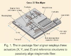
Using microactuator technology developed at MCNC and now licensed to its spinoff firm, Cronos Integrated Microsystems Inc., an in-package micro aligner (IPMA) based on MEMS technology has been designed. Boeing Co., in conjunction with Cronos, built and tested the aligner, which at 5x4x0.5 mm3 is small enough to fit into optoelectronic packages. The IPMA enables the alignment robot to be attached to the fiber-optic strand, literally moving the robot from outside to inside the package. Future development can bring the size down to as small as 1x1x0.5 mm3, which will enable multiple singlemode-fiber alignments in a single package.
Because the IPMA is small, fully integrated, and operates with low power requirements, it is a practical choice for passive alignment. The IPMA is made using micromachined silicon chips, providing both mechanical and electronic functionality. Fabricated through the process of nickel surface micromachining, each IPMA MEMS chip includes three microactuators, one each for the X, Y, and Z axis. This three-dimensional nature is an advancement over the traditional planar, two-way structure of most MEMS technologies. The actuators, which expand and contract as voltage is applied, serve as the control mechanism for the attached fiber. In addition, many active nickel structures are placed on the chip for reference, with an equivalent number of silicon circuits. These active structures can number into the hundreds for each chip.As shown in Figure 1, silicon V-grooves or electrodeposited reference structures serve to passively align the singlemode fiber to the actuators and reference structures (or benchmarks). Microlithographic patterning is used to form the structures. The equipment used in this technique has a placement accuracy of better than 0.2 micron, which is safely within the 0.5- to 0.75-micron accuracy necessary for passive alignment.
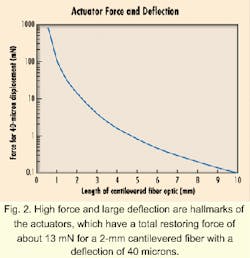
One of the IPMA's leading features is the actuators' high-force, large-deflection characteristics (see Fig. 2). Testing has revealed that the actuators must produce a minimum force of ~10 mN and yet be within specific targets for size (<5mm2 x 0.5 mm), displacement (>10 microns in one direction), force (>10 mN), and power consumption (1 W). The actuator technology described here falls safely within these critical parameters. Since the alignment function depends on the actuators' ability to perform, each actuator must be made to the specifications needed to provide enough force on its own and withstand such forces as the bending of the fiber, counterforce springs, friction, wirebonds, and the weight of the chip itself. Prototype IPMAs showed that the actuator yielded an available force of >12 mN to 60 mN at 0.3W dissipated power.If fiber bending and other forces are so significant that the actuator begins to buckle, accurate fiber alignment won't be possible. In the IPMA, counterforce springs are included to re-center the fiber in its reference position and hold the device in place during handling. These springs are designed to provide 0.5-mN force at 100-micron displacement.
Two designs of the IPMA--mounted and unmounted--have been produced. The unmounted design positions the in-plane actuators on the periphery of the fiber-holding moveable platform, connected by springs to the fixed portion. The moveable portion is first bonded into a package using standard optoelectronic placement techniques, locating the device in front of a laser diode. In addition, the laser diode is mounted on the fixed portion of the silicon substrate using passive plated-metal stops to preposition the laser in front of the fiber. Next, after the actuator is placed into the package, the lensed fiber-optic or other optical component is brought in and bonded into the fiber-holding structure. After bonding, the actuator moves to align the fiber to the laser diode.
The unmounted version of the IPMA requires a micromachined alignment cavity but is much smaller because all the actuators are on the same moveable silicon base. In this version, a separate fabrication station is used to bond the lensed fiber optic or other optical component to the silicon base. This structure then is placed into the alignment cavity in front of the optoelectronic device. After the combined fiber-optic component and actuator are placed in the alignment cavity, they can be actuated to align the fiber to the laser diode.
Placing the IPMA device into the package--in Boeing's case, the company's standard Kovar hermetic package--is the next step. After positioning the device into the package and testing for alignment, the package is sealed with Au/Sn (280C) solder. The fiber-optic feedthrough is sealed with epoxy. Inside the sealed package, the IPMA aligns the fiber-optic component to the laser diode. Coupled power level is measured with sinusoidal signals applied to each actuator to identify optimum coupling alignment.
While the IPMA has been demonstrated to work, at least one issue needs to be resolved for the self-contained IPMA to become prevalent in the singlemode optoelectronic manufacturing environment: the requirement to bond the fiber while maintaining alignment. Unacceptable loss of alignment during bonding, caused by thermomechanical effects, must be dealt with.
Several strategies are under consideration to mitigate these thermomechanical effects. Ultimately, it appears that laser welding and capacitive discharge welding of plated-metal parts will be the bonding processes of choice. These methods benefit from the close bonding of the fiber to the stage because of the extra mass the bond provides.
The final judge of whether MEMS technology can speed deployment of optoelectronic techniques is economics. With the current methods of fiber alignment--dependent on vision-recognition systems or manual sighting--economics is not kind. Every change in package or device requires a costly, time-consuming retooling in manufacturing.
The MEMS-based micro aligner has no such constraints. Retooling to change the package-specific external alignment systems is eliminated because the MEMS device is so small it will fit inside the package. This design, with its high-performance measures of force and displacement, should prove beneficial to fiber alignment.
Karen W. Markus is vice president and chief technology officer of Cronos Integrated Microsystems Inc. (Research Triangle Park, NC) and serves as chair of the IEEE-CPMT committee, Packaging Issues for MEMS and Microsystems. She can be reached at [email protected]. Robert L. Wood and Vijayakumar R. Dhuler are MEMS technologists at Cronos.

