The last few years have brought a wealth of innovation to photonic systems design and many new systems providers, breaking a tradition of conservative design rules derived by committees. Operators are now hoping to apply these innovations to extract the maximum capacity from their installed networks for the minimum possible capital and operating expenditures (capex and opex). Their new cost optimization objectives create increased complexity, so the process of link design no longer simply follows the rules.
However, the engineering cost of transferring innovations from hero experiments in the laboratory to thousands of real communications links—each of them different and most using installed fiber—must be controlled, or else the associated cost benefits will be lost.
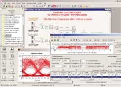
Photonic design automation (PDA) software is evolving to meet these challenges, transforming installation instructions from the theoretical into the practical. The new generation of PDA tools marks an expansion in use from the conventional simulation tools that were designed for researchers attempting to optimize cutting-edge prototypes and make them robust.Traditional PDA software was designed for almost limitless innovation.1 Typically, icons linked to numerical models of components were placed on a schematic diagram, then wired together to form a subsystem or systems simulation (see Figure 1 screenshot). The parameters of each model could be changed to represent a specific component, such as the performance of a commercial component. When run, the simulation engine would pass signals between the modules and "fire" them in an appropriate order. The output signals would then be visualized (as waveforms, spectra, eyes) or analyzed for performance metrics like Q, bit-error rate (BER), or eye-opening. Because the models represented the physics of the components and many parameters were available, the software could model almost every photonic component of interest to communications engineers. Also, because hundreds of modules could be wired together in almost any topology, any type of subsystem, system, or network could be simulated.
Unfortunately, this design methodology requires a photonic "guru" for every link design in a network, and a thorough knowledge of available equipment. This solution is not scalable, so the gurus traditionally suggest simplified design rules to the link engineering teams. But for most links, these rules will lead to overly conservative designs, meaning wasted capex or lost contracts.
However, many communications link design tasks have similar topologies such as a multichannel transmitter, a multiplexer, and identical spans consisting of fibers, amplifiers, and dispersion-compensating modules. For a long-haul span, selecting modules, wiring them together, and setting their parameters could be time-consuming. As a result, some PDA vendors introduced "wizards" to synthesize WDM designs given link specifications like transmission distance, bit rate, and fiber type. The wizards create a populated schematic by selecting modules, wiring them together, and setting parameters—in a way, they emulate keyboard and mouse actions.
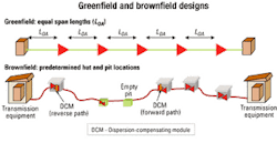
Wizards are created by capturing a "by-hand" design, using terminal control language scripting to add interactive comments and mathematical calculations. Wizards are also supplied to verify a design by taking it through a standard set of tests, starting with power analysis and ending in full nonlinear simulation.Although wizards have proven popular for automating greenfield design tasks using reasonably simple design rules, they do not fully meet the requirements of link engineers requiring brownfield designs. Brownfield designs have fixed existing plant, ready-made rights of way, or even dark fiber (see Figure 2). That complicates the design process considerably. In a greenfield design, the amplifier spacings can be constant and calculated from optical-signal-to-noise-ratio (OSNR) considerations using the "58-equation."2 In a brownfield design, amplifiers should be placed in huts or pits, whereby spacing is predefined. That becomes an "integer-programming" problem,3 whereby an integer number of amplifiers (including zero) is placed in each hut or pit. Furthermore, the type of amplifier is an integer choice, be it manufacturer or part number. The same is true for dispersion compensators and attenuators.
Integer programming, or configuration, is a complex branch of mathematics requiring much more complex search procedures than are commonly used in PDA wizards, which presume infinitely variable component characteristics to reach an optimum design. Integer programming also requires fast evaluation of trial designs, since a solution can involve hundreds of iterations of component selections. Thus, the level of detail in the component models has to be compromised for speed. Alternatively, since the application of the models is restricted to WDM links, appropriate approximations can be made without a large loss of accuracy. The definition of components must also align with manufacturers' test data and data sheets—and the presentation of results must be in a form usable by an installation technician.
Because of these key differences between PDA tools for research and configuration tools for photonic links, some PDA manufacturers embarked on a development program for a new type of PDA tool, a link configurator, which focuses on the requirements of link engineers.
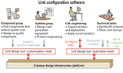
For a given brownfield specification, the tool must select the lowest-cost configuration of commercial components and present the results in a flexible way so components can be ordered, costs calculated, and installation planned. The tool serves to scale the expert knowledge of the development department and put it in the hands of the link designers, saving costs with every link design. That is achieved by allowing the guru to specify custom design strategies selected by the link designers or equipment manufacturers.The tool has two main modes of operation (see Figure 3). All users share data and results through a common design infrastructure, though they will use and view data in different ways according to job function.
In customization mode, the product expertise of the component and systems design groups is captured. The components and their characteristics are entered into a component database. The knowledge of the systems engineers is captured as design strategies. These strategies account for component interworking issues, together with proprietary design techniques and configuration rules.
Far more commonly the link design tool is used in application mode, typically by link engineers and technical salespeople, but also by engineering groups within operators for longer-term planning. A typical design process in application mode follows.The link design process has a number of stages (see left side of the graphical user interface screenshot, Figure 4). The first stage is to enter the link requirement, including link length, capacity per optical channel, BER, and total bit rate per fiber. In the second stage, the topology is entered, including existing fibers, repeater locations, and wavelength assignments of transmitters. The span engineering rules are also selected at this stage and modified for the task at hand.
The script execution stage synthesizes a number of link designs by selecting from the component database with a view to minimizing cost while satisfying other design constraints. For example, synthesis must choose the types of terminal, amplification, and dispersion compensation equipment that will meet the bandwidth-length requirements at the lowest cost, while satisfying constraints that may include heat dissipation, safe power levels, and footprint.
Intelligent strategies will use points of excess gain to insert dispersion-compensating modules or leave out amplifiers altogether. The script fills in the details of a brownfield topology (see the top of Figure 4 screenshot) with actual components (shown as icons representing the components). The algorithms rely on an "effective fiber" approach to fiber modeling, which reduces the modeling of cross-phase modulation along a fiber to a single-step calculation.
The synthesis engine ranks the designs by performance parameters or cost, presenting them as a table in comparison mode. The designs can then be investigated in interactive mode plotting the performance of each channel versus distance along the length of the link. The plotted parameters include signal level, noise level, OSNR, dispersion, cross-phase modulation, self-phase modulation, mean differential group delay, wavelength (in case of wavelength conversion), and incremental cost. Each channel can be plotted as a separate trace, or the spectra of the channel powers can be plotted at each junction of the component. Error bars, indicating margins, are also plotted. If desired, a manual design process can replace the automated synthesis by placing components from a palette. The rapid charting of the performance metrics of the link facilitates manual design, since the effects of design changes appear almost instantly. Additionally, a design can be automatically exported to a full sampled signal level simulation, which can identify subtle gains in performance from consideration of the full interactions of dispersive components and nonlinearities.
Once a final design is chosen, the results can be converted into results files. A typical file format is a bill of materials, including indicative costs. Other reports may include settings for adjustable components such as amplifiers. The report format can be customized to include introductory material and derived calculations such as a breakdown of cost versus component type.
The availability of link configuration software allows advances in the research laboratory to be applied to many thousands of link designs. Since the knowledge of component and systems engineers is captured electronically, then distributed to link engineers as design strategies, over-design can be avoided. The result is capex savings, not to mention a standardization of the design process and uniform implementation of design strategies that may include subtle design considerations.
The designs themselves are also captured electronically during the design process for reuse and, more important, future upgrades. Upgrade strategies can be examined in detail by exporting link topologies to physical layer design software for full verification at a signal level. Having all link designs stored electronically enables the full value of a network to be realized and manages the value of the network over its entire lifecycle.
Arthur Lowery is group technology officer and Rudi Moosburger is vice president of VPIphotonics (Melbourne, Australia), a division of VPIsystems.
- A.J. Lowery, "Photonic Simulation Tools," Optical Fiber Telecommunications IVB (Chapter 12), I. Kaminow and T. Li (Eds.), Academic Press, San Diego, 2002.
- J.L. Zyskind et al., "High-Capacity, Ultralong-haul Transmission,", Optical Fiber Telecommunications IVB (Chapter 5), I. Kaminow and T. Li (Eds.), Academic Press, San Diego, 2002.
- G.L. Nemhauser and L.A. Wolsey, Integer and Combinatorial Optimization, Wiley-Interscience, New Jersey, 1999.


