Today, MEMS is the word in components for the all-optical network, but will traditional silicon-based MEMS technology always fit the bill?
MIKE LITTLE and BEN JAMISON, Solus Micro Technologies
It's no secret that tremendous growth of the Internet and burgeoning telecommunications traffic are causing severe congestion in the overall network structure. To address the ever-increasing need for bandwidth and agility, networks will continue to grow in size and complexity.
As service providers eagerly look for new ways to generate revenue and lower operating costs, many telecom companies are deploying WDM and DWDM network topologies and transport technologies to boost the efficiencies of their networks. Currently, much of today's telecom infrastructure is based on a foundation of optoelectronics equipment. Because of the bottlenecks created by optical-to-electrical conversions in today's network, industry experts agree that most of the electronics will be taken out of network signal processing and routing applications and replaced with more efficient optical technologies that are protocol-independent and have much higher bandwidth and wavelength agility.
With the advent of fiber-optic networks-a major part of the unprecedented growth in communications systems-the deployment of all-optical networks is clearly the ultimate goal for the next generation of telecom networks. But for very agile all-optical networks to become a reality, increasing carrying capacity and wavelength tunability are critical elements. That requires development of terabit routing and very flexible wavelength routing devices such as optical crossconnects, optical multiplexers, and wavelength translators.
Recently, micro-electromechanical systems (MEMS) technology has received widespread attention for a very broad assortment of applications, from airbag sensors to display devices. MEMS are an outgrowth of integrated-circuit (IC) technology; semiconductor-processing equipment is used to build a wide variety of tiny mechanical structures. The IC industry's ability to deposit, pattern, and etch micron-scale features in silicon, SiO2, and aluminum has been exploited to build tiny sensors such as accelerometers and gyros as well as "actuators" as diverse as gears and micro-mirrors.Optical networking has become an application for this technology only during the past year or two, tied to the ever-increasing demand for faster and better ways to transmit information. MEMS technology supplies electronic systems with a much-needed window on the physical world, permitting them to sense and control light, motion, sound, heat, and other physical forces, making it ideal for developing optical-networking products for the 21st century.
The most recent industry research forecasts sales revenue for MEMS optical components to be in excess of $20 billion by 2004, with continued strong growth throughout the next decade. Clearly, MEMS is regarded as an essential technology for improving the performance and efficiency of all-optical networks as well as a means to reduce costs.
A number of revolutionary MEMS telecom products has recently emerged from the laboratory into real world applications. These devices are fabricated using traditional MEMS materials (silicon-based) and processes derived from the IC industry. Unfortunately, most silicon-based materials have roughly similar mechanical properties, and the technology used to deposit layers of these materials limits their thickness to no more than a few microns. That in turn limits the design space for MEMS devices.
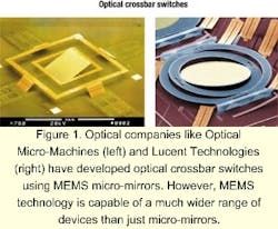
In the telecom area, the most publicized application of MEMS is for optical crossbar switches (OCXs), which are an essential element of all-optical networks. Several startups as well as large established companies have embarked on developing an OCX based on MEMS micro-mirrors (see Figure 1).
The spring hinges that form the gimbal supports for these micro-mirrors are fabricated of silicon, which is a very rigid material (high Young's modulus, ~160 GPa). The high rigidity of silicon, coupled with the requirement to operate the micro-mirrors at moderate voltages, forces designers to use very thin, delicate structures for the spring hinges, often barely visible in the photomicrographs.
Recently, a new class of MEMS devices started to surface-components made with highly compliant polymeric materials as a principal design element. Typically in MEMS devices, electrostatic or piezo forces are used to bend or deflect one of the MEMS layers to produce the desired mechanical motion. Stiffer materials require higher voltages to achieve a given mechanical deflection, and traditional silicon-based materials are all extraordinarily stiff.
The compliant MEMS (CMEMS) technology platform differs from conventional MEMS by adding a set of softer, more compliant polymeric materials to the list of conventional rigid silicon-based materials used in MEMS. Adding these compliant materials to the list of substances that can be deposited, patterned, and etched greatly widens the design space.
The compliant materials used in this new class of MEMS devices are as much as six orders of magnitude less stiff and can be easily tailored over a range of three orders of magnitude. Additionally, they can be deposited in a much broader range of layer thickness. This very wide range of flexibility expands the design space for MEMS devices far beyond what is possible with traditional silicon-based materials.
This CMEMS platform enables the development of components and assemblies that demonstrate superior performance and lower costs compared with using the silicon-based MEMS solutions currently available. Its unique architecture is ideal for a broad range of high-performance tunable photonic components demanded by the telecommunications industry, where it offers several significant benefits over traditional MEMS-based designs.
One such component is the tunable optical filter (or interferometer). Tunable-filter technologies are used in many optical-networking applications. While an interferometer may be achieved using a number of different methods, the most commonly used is the Fabry-Perot-based tunable filter.
Fabry-Perot filters generally are divided into one of two basic categories. In the first, the distance between the parallel plates is controlled to tune the wavelength that will pass through the filter. Piezo control is most typical. Newer interferometers have employed silicon MEMS technologies to control the separation between the plates.
This type of device typically has difficulty maintaining the necessary tight tolerance on the parallel orientation of the plates. Doing so is complex and expensive. Furthermore, piezo devices, in addition to requiring high voltages, have a relatively narrow operating-temperature range. The voltage and thermal requirements of the piezoelectric devices impose difficult and labor-intensive manufacturing and assembly operations, adding cost to the devices and making them less reliable.The second category of tunable filters uses fixed parallel plates and tunes the refractive index of an electro-optic material that fills the cavity between the plates. When voltage is applied, the refractive index changes. Typical electro-optic devices use lithium niobate or liquid crystal and require unreasonably high voltages to achieve a tiny fraction of the desired tuning range. The small value of the electro-optic coefficient is responsible for the high voltage and insufficient tunability, leading to large, bulky devices.
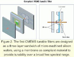
The first CMEMS tunable filters are designed as a three-layer sandwich of micro-machined silicon wafers (see Figure 2). The first layer is a silicon substrate with a high-reflectivity dielectric mirror on its interior surface and a high-efficiency, antireflection coating on its outside surface. The second layer contains the high-reflectivity movable mirror that is the tuning element of the Fabry-Perot filter. It has a high-reflectivity dielectric mirror deposited on a silicon island suspended from a perimeter frame using a compliant polymer layer.
Segmented electrodes on the backside of the polymer layer match up with electrodes contained on the third and final layer. Voltages applied between the second and third layers control the gap between the first two layers, while the segmented electrodes enable precise adjustment of the Fabry-Perot cavity.
The tunable Fabry-Perot shown in Figure 2 is a three-piece MEMS design that uses a unique compliant membrane to support a movable mirror. Voltages applied to the backside electrodes provide precise control of the gap between the mirrors.
As noted earlier, the emergence of DWDM and all-optical networks has created the need for a number of tunable devices. Key among these is the optical performance monitor (OPM). As network providers move toward higher data rates and denser channel spacing-allowing use of hundreds of channels in a single fiber-performance monitoring becomes increasingly critical. The more wavelengths crowded together, the greater the chance that individual optical signals will be lost or degraded. For a service provider, that can be a financial nightmare to the tune of up to $10,000 per minute per channel!
Thus, a pressing need currently exists in DWDM networks to measure, in the optical domain, the performance and health of all channels on a fiber. The vital element of the OPM is the tunable filter that must select the desired DWDM channel for quality measurements such as power, signal/noise, and actual wavelength.
CMEMS technology is very robust and elegantly simple in its design, making it both reliable and less expensive than the alternative solutions available today. Its first application is in a new tunable Fabry-Perot filter-currently being developed for the OPM market-that uses an elastomer to suspend the movable mirror. This design offers better performance, higher yields, and lower costs than those fabricated with conventional silicon-based materials.
There are several other advantages that CMEMS technology enjoys over silicon-based MEMS:
- Mechanical deflection requires much lower voltages.
- Mechanical range of motion is much larger for equivalent voltages.
- Mechanical damping can be included to avoid high-frequency noise.
- Spin-on deposition techniques can simplify processing and lower costs.
- Less precisely defined geometries can lower costs and improve yields.
- Fewer discrete components provide better reliability at lower cost.
- Compact package design permits superior integration.
These advantages allow very-high-performance tunable-filter characteristics that result in:
- Very high finesse characteristics for superior channel selectivity.
- High filter contrast (40 dB) for precision measurements of optical power and signal/noise ratio.
- Low insertion losses.
As the telecommunications industry continues to move toward denser, higher-bandwidth all-optical networks, the need for tunable components that enable new levels of functionality and performance becomes more urgent. The anticipated success of CMEMS technology will undoubtedly set the stage for their use in other optical-networking products such as tunable lasers, multiplexing/demultiplexing filters, gain-flattening devices, and add/drop multiplexers. Additional applications may also include tunable dispersion compensation devices and any number of tunable components designed to significantly reduce the need for frequent signal regeneration and increase the agility of the optical network, while substantially lowering both capital and operating expenditures.
Mike Little is chief technical officer and Ben Jamison is vice president of marketing at Solus Micro Technologies (Westlake Village, CA). They can be reached via the company's Website, www.solustech.com.
Address letters to:
Letters to the Editor
Lightwave
98 Spit Brook Road
Nashua, NH 03062-5737
e-mail to:
[email protected].
Include daytime telephone number. Letters may be edited.

