Is photonic hybrid integration the way to go?
As the industry wrestles with a solution to monolithic optical integration, hybrid integration may provide the next logical step in the integrated manufacturing of photonics.
By GARY M. KAYE
Over the course of more than a half-century, the process of manufacturing electronic components has moved from those early tubes and capacitors laid out on punchboards to today's silicon wafers with millions of transistors on a single chip. A key enabling technology for the advancement of electronics manufacturing from discrete components to integrated circuits was the use of silicon as the common building block.
For the photonics industry, there is still no clear path to fully integrated manufacturing-there is no universal material system for optics. Photonic components are crafted from a variety of materials. Although silicon is a common base material for micro-electromechanical systems (MEMS) switches, active devices such as lasers and semiconductor optical amplifiers are typically manufactured structures that have been epitaxially grown on indium and gallium arsenide. Spectral filters are typically manufactured from thin-film stacks of silicon dioxide, tantalum pentoxide, and titanium dioxide, whereas crystals such as rutile and garnet are commonly required for polarization control and isolation.
To date, optical component and subsystem manufacturers are still in search of truly integrated manufacturing, but there have been strides made in hybrid manufacturing, combining multiple optical components in a single package. Two technologies have been employed to move light from one component to another: optical waveguides and free-space interconnect. Neither offers a perfect solution.The advantage to waveguide manufacturing, such as that used by Bookham Technology and Kymata, is that it has fewer surfaces, and the waveguides resolve many of the alignment problems inherent in putting together arrays of components. There are several drawbacks to waveguides, however. Because waveguides cannot make tight, low-loss turns or easily cross over, the packages are inherently larger than their free-space counterparts, which can achieve a low-loss 90-degree turn with a simple fold mirror.
The limits of how light bends (or doesn't bend) in a waveguide forces the manufacturer to do the same kind of engineering that railroads must perform in building a train trestle with a maximum 6% grade. Here again, giving the light room to bend also requires more space within the package. Moreover, one of the most attractive features of light is the ability of multiple beams to pass through the same space without mutual interference-this capability is lost with waveguide systems.Finally, another significant drawback to waveguide technology is the problem of coupling. Every time waveguides are coupled to each other, there is light loss. Given the technical challenges of signal amplification in photonics design, this signal loss can become a significant factor in complex photonic subsystems.
To avoid some of the problems inherent in waveguide manufacturing, companies such as AXSUN Technologies, Lucent Technologies, Nortel Networks, and Digital Optics have turned to free-space interconnect designs. In such systems, beams can freely cross one another. Mirrors can be used to turn light at sharp angles without signal loss. As a result, free-space photonic packaging can be inherently smaller. Because light moves around unguided, there is no internal waveguide signal coupling loss.
However, free-space manufactured designs are not without their own challenges. Because there are so many optical surfaces within a free-space package, there is the potential for light to go astray, so thin-film antireflective or highly reflective coating technology becomes a major factor in successful free-space packaging design. Other key issues are the availability of high-performance versions of the bulk optical elements required and the need for special equipment and processes to precisely mount the elements to a suitable optical bench.
Perhaps even more critical is the matter of precision alignment. Because there is nothing physically forcing the beams of light to move from component "A" to component "B," alignment of components to submicron alignment tolerances is critical.
In one example, a variety of manufacturing techniques are being combined in an effort to speed the process of automated photonics manufacturing, while at the same time reducing the size and cost of photonic subsystems. This hybrid-integration platform utilizes a variety of microelements attached to a substrate using advanced solder-joining and precision-alignment processes, interconnected with free-space optical beams.
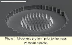
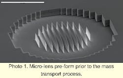
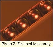
A proprietary mass-transport lens technology has been implemented to make lenses at the wafer scale in the same way integrated circuits are made (see Photos 1 and 2). With thin-film optical coating technology, a wide range of refractive and reflective optics (a millimeter or smaller) can be fabricated at relatively low cost.The mass-transport process and subsequent proprietary improvements to this process (both licensed and patented) allow production of a wide range of lenses and lens arrays for passive and active devices. Thousands of individual lenses are fabricated in parallel on a single wafer. In the case of lens arrays, the relative placement of lenses is determined with lithographic precision. The passive alignment structures used in subsequent hybrid assembly steps can be included on the lenses, as well.
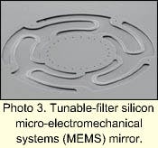
Semiconductor fabrication technology is also used for other so-called MEMS components such as tunable filters and optical switches, which add optical-layer functionality and value to photonic subsystems. Photo 3 illustrates a tunable filter that is a MEMS version of the common tunable Fabry-Perot interferometer.
To achieve precise alignment of the components, a customized bonder installs each element on a micro-optical bench within the photonic package. Initially, passive alignment is performed to tolerances greater than a micron, which will be subsequently refined during the active alignment process. This step is of critical importance in semiconductor-based optical-system manufacturing.
Consider the specific example of coupling a semiconductor diode laser, such as a pump laser, to a fiber core of a singlemode fiber. Only the power coupled into the fiber core is usable to optically pump a subsequent gain fiber, such as a rare-earth doped fiber or standard fiber, in a Raman pumping scheme. The coupling efficiency is highly dependent on accurate and stable alignment between the laser output facet and the core of the fiber; inaccurate alignment can result in partial or complete loss of signal transmission through the optical system.
Moreover, such optical systems require mechanically robust mounting and alignment configurations. During manufacturing, the systems are exposed to wide temperature ranges, and product specifications can explicitly require temperature cycle testing. After delivery, the systems can be further exposed to long-term temperature cycling and mechanical shock.Solder joining and laser welding are two common mounting techniques. Solder attachment of optical elements is possible by performing alignment with a molten solder joint between the element to be aligned and the platform or substrate to which it is being attached. The solder is then solidified to "lock in" the alignment. In the case of laser welding, the fiber, for example, is held in a clip that is then aligned to the semiconductor laser and welded in place. The fiber then may also be further welded to the clip to yield alignment along other axes. Secondary welds are often employed to compensate for alignment shifts due to the weld itself, but as with solder systems, absolute compensation is not possible.
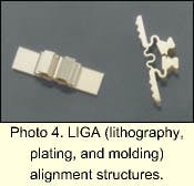
To facilitate the active alignment process, this hybrid process utilizes micro-alignment structures manufactured by a bulk MEMS technology known as LIGA-a German acronym that stands for lithography, plating, and molding. These structures, as shown in Photo 4, which look like very small brackets, are used to mount optical elements such as lenses to the optical equivalent of a circuit board, termed a micro-optical bench. The LIGA structures offer multiple degrees of freedom to enable alignment for elements such as fibers, lenses, and mirrors, while providing stable mounting surfaces and highly stable support structures.Again, semiconductor manufacturing techniques are used to create the LIGA structures. But since the LIGA structure is metal, not silicon, it is fabricated using X-ray lithography and metal plating. A bonder positions the LIGA structure on the bench substrate during the initial manufacturing process. The bonder system uses machine vision and pick-and-place software to position and attach the elements, without the need for external alignment signals. During this process, components are attached with tolerances of approximately 1 micron.
In the final active alignment phase, a micro robot is then used to perform final submicron alignment. Here, the micro-robot tools will use a "figure of merit" signal derived from an optical measurement to monitor and optimize the critical alignment between two or more elements.
Once the photonic hybrid "circuit" is assembled, it still needs to interconnect with the rest of its world, an interface to external systems and environments. That means hermetically sealed feed-throughs for the optical signals as well as electrical interfaces and effective temperature control using a thermo-electric (TE) cooler. Here too, the size advantage for the hybrid package allows the integration of multiple elements into a single enclosure, where more traditional, discretely packaged devices might require multiple enclosures and multiple TE coolers.
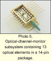
In the final analysis, the hybrid-packaging platform allows the rapid manufacture of complete hybrid subsystems such as the optical-channel monitor (see Photo 5), in which 13 optical elements are integrated within a 14-pin butterfly enclosure that typically had been used for a single component such as a laser diode. Automated hybrid systems hold the promise of helping component manufacturers add functionality and reliability, while reducing not only the cost of acquisition but also the total cost of ownership.
Gary M. Kaye has been a journalist for more than 30 years, the last 15 specializing in high technology. He has been a contributing editor for Photonics Spectra magazine and a technology producer for ABC News and CNN, among others. This article was written for AXSUN Technologies (Billerica, MA). He can be reached at the company's Website, www.axsun.com.
