By RUDY PRATER and ROB HANNAH
The lower cost of SFP+ modules comes at the cost of increased engineering complexity for systems designers.
Traditionally, 10-Gbps transceiver implementations have used two approaches to ease host board design constraints. In the first, the data is retimed to re-establish a clean clock in the data stream with minimal jitter. In the second, the data stream is converted from a serial data path at the full bit rate to multiple data paths with lower clock rates. These techniques, however, increase power dissipation and system complexity. Traditionally for 10-Gbps transceivers, this extra complexity was built into the module, increasing unit costs significantly.
The SFP+ platform modifies the allocation of these elements between the transceiver and the host to minimize overall costs. However, this architecture change puts a greater burden on the host system designer, who must design the electrical transmission channels with greater care and discipline than has been necessary for systems operating at 4 Gbps and below.
CDRs and SerDes
The major change between SFP+ applications and those using SFP modules is the increased difficulty in designing the systems' electrical signal path. Even when using the enhanced grade of FR4 PCB material, the rate of signal degradation during propagation down even well-designed differential pair traces is significant.
As with previous evolutions of transceiver form factors, the decision about how and where to implement the necessary protocol functional blocks has been changed for SFP+.
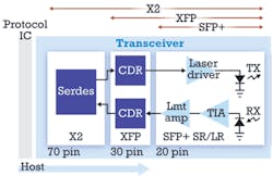
The additional functions that are frequently used at data rates greater than 4.25 Gbps between the optical channel and the basic functions accomplished by the host system (i.e., the retiming and the conversion to lower-rate parallel bit streams) are accomplished through the clock and data recovery (CDR) and through serializer/deserializer (SerDes) functional blocks (see Figure 1).
The first generation of 10 Gbps transceivers included these functions inside the transceiver, as indicated in Figure 1. Unfortunately, this implementation, while technically feasible, required that the transceivers have:
- a wide electrical connector to accommodate the parallel bit streams (limiting the achievable port/count density)
- relatively high power dissipation (creating thermal challenges)
- perhaps most importantly, relatively high cost (which limited the adoption of 10G interfaces).
The second generation of 10-Gbps transceivers moved the SerDes function outside the module onto the host board. Here, it could be integrated with other system functions more efficiently, decreasing the electrical power required by the transceiver and enabling a smaller connector interface and overall physical footprint. The internal CDR ensured that the high-speed electrical signal at 10 Gbps was retimed inside the transceiver, eliminating some of the accumulated signal degradation before it reached the host board.
The SFP+ platform progresses to the next level, moving the CDR function to the host, as well. This change enables a significant reduction in the size of the transceiver electrical connector/housing, as well as a further reduction in power dissipation. The attendant overall cost reduction also has promoted SFP+ adoption.
Yet, as mentioned previously, these architecture changes mean a tradeoff between leveraging the benefits of the SFP+ and the considerably greater level of care required in designing the host board signal paths.
LRM applications and the SFP+ linear interface
Designs for 10GBase-LRM applications face an additional twist. To support 300-m reach over legacy multimode fiber, 10GBase-LRM calls for the use of electronic dispersion compensation (EDC). The EDC function generally is realized in PHY integrated circuits that reside on the host board. Since the EDC has been engineered to correct signal degradation with very specific characteristics that are expected from the propagation of the optical signal in the fiber, the EDC circuit needs to receive an accurate representation of the optical signal incident on the receive detector.
Specifically, the amplification of the optical signal representation from the photodetector must be very linear so that a faithful representation of the received signal is processed by the digital filter. While some additional degradation from the transmission of the electrical signal through the RF traces and the module connector will also be corrected, the lower the amount of additional degradation present, the more easily the filter can adapt to correct the optical path degradation.
The end result is: the better the design of the signal path in the transceiver–but especially the design of the generally longer traces on the host board–the better the performance of the entire link. While this statement is true for SR and LR links as well, the quality of the PCB RF design is especially important for LRM links.
New challenges in testing
Systems implementing SFP+ at 10-Gbps data rates are vulnerable to poor link performance that results when inadequate care is taken in the design of the electrical channel on the host PCB.
The SFP+ MSA identifies limits for 10-Gbps trace lengths at 200 mm (8 inches) using enhanced-grade FR4, and 150 mm (6 inches) using standardgrade FR4. While these limits could be longer in 8.5-Gbps designs, pushing this limit too far can increase project costs through added debug time and PCB changes, if performance does not meet expectations.
Whereas trace length is an easily quantifiable metric, many other geometric factors also influence signal integrity. It is a significant challenge to keep the paths between the SFP+ connectors and the PHY IC within spec for all ports in a high-density host design, as well as to find the optimum geometry for each port.
The interface between the transceiver and the host system needs more careful definition at these data rates and, when a design is not working, it is important to be able to isolate clearly which part of the system is causing a particular issue.
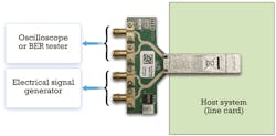
The primary method for quantifying the host channel design performance is the measurement of the system's S-parameters. To this end, the MSA has defined some standard test conditions and test fixtures (see Figure 2) so that a meaningful, well-defined test can reasonably compare one system to another, not to mention assist in isolating the weakest element in the system when performance is sub-par.
S-parameters are fundamentally a measure of the effective impedance of a circuit as a function of frequency. The MSA, therefore, specifies a maximum value as a function of frequency. The measurements can seem abstract and difficult to those unaccustomed to them, but they are actually straightforward with the appropriate equipment, as long as proper care is taken to calibrate the measurement according to the instructions of the equipment manufacturer.
Figure 3 shows the results of such measurements. Note that the S-parameters specified are differential S-parameters, characteristics of the energy transmitted along the differential pair of traces on the PCB. The differential S-parameters can be constructed from measurements of the single-ended S-parameters made on each trace separately.
The other major change in testing SFP+ systems arises from the need to use more advanced signal processing on the electrical signals in the host to compensate for propagation degradation while traversing the system's electrical channel.
For example, on the optical transmit side, the host system component may employ pre-emphasis when launching energy into the electrical channel that feeds the optical transmitter in the module. On the receive side of the transceiver, compensation is useful as well. Some transceivers have an optional pre-emphasis built in to the receive channel output, but many do not. For these transceivers, post compensation or equalization can be applied by the next stage in the system, the PHY integrated circuit that performs the SerDes function as well as protocol coding. Equalization compensates for the static characteristics of the copper traces on the PCB and the effects of the SFP+ connector. Equalization uses a subset of the same technology as the EDC required for the LRM standards. The 10G systems, thus, have the additional design issue of switching the operation of the PHY circuit, depending on whether an LRM module has been inserted as opposed to an SR or LR transceiver.
The primary disadvantage of this new reliance on signal processing techniques, beyond increased system complexity, is the impact on testing and debugging the system. The extreme case of this effect is that the LRM transceiver has specifications to define performance when operated as a standalone device that can seem abstract and unintuitive. The standard quality benchmark for modules–receiver sensitivity at 8 Gbps and below and stressed receiver sensitivity for 10GBase modules–holds no meaning for a standalone SFP+ LRM transceiver. This benchmark can only be used to characterize a link that includes the EDC function.
For a meaningful measure, three parts of the link are critical:
- the transceiver
- the PHY IC with EDC
- the exact layout and configuration of the copper traces in the transceiver but, more importantly, on the host PCB.
While the SFP+ LRM receiver offers an extreme example of the effects of electrical signal processing on testing and debugging, the same issues pertain to the receivers in SFP+ SR and SFP+ LR modules, if less severely.
More troubling can be the influence of the application of preemphasis to the electrical input of the transmitter. Qualitative judgments are often made about transmit performance, and these can be strongly influenced by the pre-emphasis of the signal applied to the transceiver input pins. The shape of the eye can change significantly, depending on the signal characteristics at the SFP+ connector. Attempts to quantify these effects are necessary, using either mask margin or a variety of jitter measurements. These also will vary significantly with different pre-emphasis settings, if only because the shape of the eye affects the choices for the 1 level, 0 level, or the level on the edge where the jitter is measured. These measurement points are often implicitly determined by the test equipment, but it is important that the test engineer be aware of such issues and use appropriate skepticism and care when drawing conclusions from the data.
From the system design perspective, choices have to be made that are often somewhat arbitrary. These include whether a single TX emphasis setting is sufficient for all ports and all modules or whether some variation in the emphasis settings should be made to depend on each particular port's layout geometry. Another possible refinement might be to vary the pre-emphasis settings according to either transceiver type, transceiver manufacturer, or both.
It is important to realize, however, that the correlation between small variations in mask margin or jitter and performance over a worst case link is not obvious. While it is clear that the extreme values for mask margin and jitter lead to poor link performance, the sensitivity of system BER to commonly seen tolerances for these values is not obvious and, unfortunately, not easy to test.
In summary, the effects of pre-emphasis and equalization are significant and complicate system testing, qualification, and system debugging for SFP+ links in ways not generally experienced with prior data rates. The interaction between the various components of the system, especially including the design of the RF copper connections, are quite likely to be the source of more performance issues than the performance of any isolated component. Thus, more care will be needed for disciplined, quantitative approaches to testing and debugging.
RUDY PRATER was a senior applications engineer in the Fiber Optic Products Division of Avago Technologies at the time this article was written; he is no longer with the company. ROB HANNAH currently is applications engineering manager at Avago.


