Increases in IC processing power have followed Moore's Law—doubling roughly every 18 months. But while the number of transistors in mainstream microprocessors has increased by 1,000 times over the last 20 years, the amount of data input and output (I/O) has increased by only about 10 times. Moreover, since the speed within chips has also grown much faster than the signaling rates between chips, overall on-chip bandwidth has grown 10,000 times faster than off-chip bandwidth.
This I/O discrepancy exists because cost-effective, electronic printed circuit boards don't support high-speed signals well over distance (what is known as a "limited distance-bandwidth product"), and routing and managing many high-speed signals on chip packages and then over planar circuit boards is increasingly complicated and expensive. The I/O bottleneck results in mainstream systems that are built with fast chips; slow, short buses; and few chips per board, connected to the "network" by a slow link. These limitations will only worsen with time.
Optical connections, by contrast, do not have the same distance-bandwidth problems; routing with fiber is done easily. In addition, optical packaging complexity does not scale in difficulty with increasing data rates or with the number of I/Os in the way that electronic packaging does. Therefore, if the chip I/O could be converted from an electrical to optical data stream, the above architectural problems are circumvented. In other words, significant enhancements in system performance and scalability can be achieved by moving optics as close to the electronic chips as possible.
This type of optical data transfer has been too difficult to achieve with conventional optical connections. In particular, such optical approaches have not had the channel count to handle the larger number of data I/O lines that electronic chips have possessed. While electronic chips have utilized dozens to hundreds of data I/O lines, optical devices have been limited to 12 I/Os or less. Moreover, traditional optical modules themselves contain large numbers of chips and would in many cases have been more expensive than the electronic chips for which they were to provide I/O.
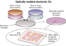
Today, however, wafers bearing industry-standard optical devices such as top-emitting vertical-cavity surface-emitting lasers (VCSELs), distributed Bragg reflector (DBR) lasers, photodetectors, or other devices consisting of compound semiconductor materials can be integrated directly with silicon electronic IC wafers to create "optically enabled electronic integrated-circuit" wafers. The result is electronic chips with large quantities of optical devices fused to them for I/O (see Figure 1). Compressing optical systems to individual chips creates a low-cost, high-performance, very scalable method to obtain optical I/O. Dozens to hundreds to thousands of optical I/Os can be achieved with a low marginal cost. By packaging such chips, optical I/O is moved as close to the electronics as possible.This approach has been used in products currently sold as a transceiver—which is just a packaged version of such a chip. Transceiver products containing 72 I/Os (36 transmit and 36 receive) with data rates of up to 5.6 Gbits/sec per I/O (giving 400 Gbits/sec of overall bandwidth) have been developed.
Yet, while an optically enabled transceiver IC has been the first commercially released product incorporating this technology, the same integration approach works equally well for any type of chip. The base electronic chip could include any type of higher-level functionality, from memory to a network processor or microprocessor.
As an interim step between optically enabled transceiver ICs and optically enabled higher-level function ICs, a two-chip package has been implemented to provide optical I/O as close as possible to existing ICs without actually integrating the optics onto the higher-level IC. In such a scenario, the package contains two chips, an optically enabled transceiver IC and a conventional IC. I/O is also be capable of being sent out of the two-chip package optically, providing the greater distance-bandwidth product and eliminating the need to route signals on printed circuit boards. By reducing the optics to one chip, the lowest-cost solution for optical I/O can be made while still maintaining the flexibility of applying this solution to any chip currently in the marketplace.
The first products taking advantage of this two-chip integration contain electronic crossbar chips as the higher-level function chips. A crossbar chip can access a number of input and output data lines and internally reconfigure which input lines are connected to which output lines. By tightly integrating optics, the chips can now take each of those inputs either electrically (as they did before) or optically (see Figure 2).By providing optical-I/O capability, these optically enabled crossbar switch chips can now be operated in a number of ways. First, the chip can be used in a pure electronic mode in which electronic inputs route to electronic outputs and the optical signals are ignored. In essence, it could be used as a simple electrical crossbar switch—as they traditionally would be used—meaning that an optically enabled chip would still allow the chip to operate in existing systems as it always has. Second, these chips could be operated in a pure optical mode in which optical inputs would route to optical outputs and the electronic I/O would be ignored. In this mode, the chip would be a fully optical crossbar. Third, the chip could be run in such a way that signals would only go from optical to electrical or electrical to optical-optical-optical or electrical-electrical routings would not be used. In this case, the module would act as an optoelectronic transceiver in which input electrical signals could be shuffled through a crossbar before exiting on the optical output and the input optical signals could be shuffled before exiting on the electrical output lines.
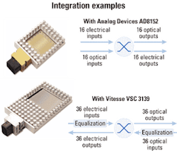
Finally, the most generic case is essentially a combination of the first three cases. In this situation, all connections of optical and electrical I/O can occur. The chip would be a crossbar switch in which a number of I/Os are provided and some of each of the I/Os are optical and electrical. That would allow additional functions like a channel add/drop capability in which a number of optical signals could enter the chip; some of them could be dropped electrically while the rest would be passed through optically. The dropped channels could then be replaced with new inputs that would enter the module electrically and exit optically on the channels that were dropped.Examples of such integration with an Analog Devices and a Vitesse crossbar switch chip are shown in Figure 3. In the case of the Analog Devices chip, the device enables 16 electrical and 16 optical inputs and 16 electrical and 16 optical outputs to occur simultaneously. In the case of the Vitesse chip, there are 36 electrical and 36 optical inputs and 36 electrical and 36 optical outputs. These modules are packaged to use a single standard MPO-style fiber connector for the optical I/O and dissipate about 8 and 10 W, respectively, including all the power dissipated by the electrical chip and optically enabled IC.
But as mentioned earlier, this approach is not limited to crossbar switch chips. Any chip that has data I/O can be packaged in the same way. By providing packages compatible with the pin-outs currently used on the higher-function chips, systems can be expanded with little or no redesign of boards, chips, or chassis. These packaged chips can be used on existing boards in an electronic-only fashion and have the added optical-I/O capability to transmit data over much farther distances.
While the two-chip packaging approach allows existing commercially available, optically enabled transceiver ICs to address the I/O needs of any existing electronic IC, future cost, power, and size reductions will occur as these two-chip packages migrate to one-chip packages. Here, the individual higher-level functional chips themselves will be optically enabled, eliminating the need for the separate transceiver chip. Whether with two chips or one, by providing large-channel-count optical I/O to any electronic chip, every chip can become a nexus between optical and electronic buses and leverage the advantages of each.
John Trezza is chief technology officer and president of Xanoptix (Merrimack, NH).


