Optical-chip platform combines liquid crystals with nano-structures
VOA integration has been made possible by MEMS, planar technology, and now even smaller, nano-enabled liquid-crystal-based optical chips. These millimeter-scale chips are diced from a laminate of glass wafers with nano-structure polarizers and other deposited thin films. The active element is a liquid-crystal (LC) layer one-10th the thickness of human hair that requires very low current and low voltage control. Such elements have proven to be robust over billions of cycles and withstand extreme manufacturing and operating environmental conditions.
Wafer-level integration of recent manufacturing improvements in subwavelength nano-optical elements expands the range of device functions the optical chip can achieve, while breakthroughs in LC manufacturing methods and the resulting performance enhancements improve upon existing uses and enables consideration of new applications.
While there are a number of dynamic actuators whose properties can be changed with the application of an electric or magnetic field, such as lithium niobate, silicon, garnet, and MEMS, LC has a number of properties that make it superior for specific applications. Possibly the most important characteristic is the change in index of refraction (Δn), which is up to 0.27 for select types of LC readily available today. When this property is induced by the application of voltage in a nematic LC cell via a layer of indium tin oxide (ITO) on the inside face of the wafer substrate, either the rotation/retardance of a specific polarization, the effective path length between optical elements, or a change to the index of refraction can be exploited to induce the desired affect.
Even a Δn of 0.2 and lower will exhibit enough range to create a superior optical-processing chip. In the case of a variable optical attenuator (VOA), that can mean attenuation levels >40 dB. For a tunable filter, that can mean a range that covers the entire C-band. Only low voltages, typically <5 V rms, are required to achieve broad performance ranges in –5° to +75°C operating environments. Another strength of liquid crystal is the ability to accept very fine resolution changes predictably and repeatedly without susceptibility to shock or vibration.
LC actuators have been designed into a number of volume-manufactured optical components and modules in recent years. However, some of these devices have displayed some lingering shortcomings, largely due to the construction methods used and expertise based on less stringent LC display requirements. High manufacturing temperature requirements, small device size and the attendant precision demands, and repeatability over component lifetime in extreme temperature and humidity have limited the use of LC actuators. Fortunately, recent breakthroughs have overcome these challenges.
Although the successful production of any LC device involves such well-known considerations as tight mechanical tolerances and contaminant-free cleanliness, applications within optical modules for telecommunications have additional requirements not met by LC display manufacturing methods. One of the critical issues is the high temperature involved in subcomponent soldering processes and hermetic sealing, where requirements sometimes exceed 200°C. That can be a particular issue with LC as it transitions into a liquid state above 100°C.
Therefore, special LC chip designs are needed to ensure that performance parameters are maintained upon cooling to typical operating conditions. Recent proprietary technology breakthroughs have shown success past 230°C, allowing LC optical chips to be used in most any butterfly-package manufacturing procedure. Long-term tests beyond 2,500 hours at 85°C have shown stable optical performance in all areas, ensuring stringent Telcordia high-temperature storage tests are surpassed.
Size is another critical barrier to incorporating additional optical elements into increasingly smaller packages. Common applications within laser source packaging dictate optical-chip outside dimensions of 2–3 mm with 1-mm depth along the optical path to maintain existing subcomponent layout and coupling efficiencies. Previous LC-based alternatives required die-level alignment and bonding of polarizer substrates to the front and back surfaces of the LC cell, since wafer-scale polarized substrates did not meet the extinction requirements for critical optical applications. As a result, previous devices were twice their potential size, required labor-intensive individual device processing, and suffered from higher cost and performance inconsistency.
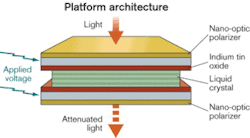
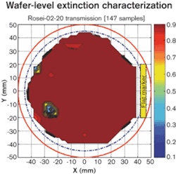
Alternative technologies such as planar-lightwave-circuit (PLC) waveguides enjoy the wafer-scale benefits but suffer from prohibitively high power consumption, high insertion loss, limited attenuation ranges, and excessive length. Mechanical solutions such as MEMS also suffer from excessive length while adding vibration and shock sensitivity, plus repeatability and durability challenges. Fortunately, recent breakthroughs in subwavelength optical elements and wafer scale nano-manufacturing enable a new type of optical-processing chip. Integrating these two technologies with the latest LC actuator technology creates a voltage-controlled VOA that is only 1 mm thick with >35-dB range, <0.6-dB loss, and <20-mW power consumption (see Figure 1).Such a VOA enables a new range of integration possibilities for devices such as optical transceivers, transponders, and tunable lasers. To fully benefit from wafer-scale manufacturing efficiencies, the nano-optic polarizers along with antireflective coatings, patterned electrically conductive ITO, and other wafer treatments are applied to the entire wafer flat, two of which are then aligned and fused. Wafer-level characterization of the optical properties are made before dicing, so poorly performing devices can be identified prior to final processing steps, avoiding costly testing and handling challenges of millimeter-scale individual devices (see Figure 2). Each wafer pair contains several hundred of the resulting transmissive optical-processing chips. Exact dimensions are easily customized to meet specific application requirements.
Nano-optic effects are the result of the transmissive and reflective properties of structures with customizable nanometer-scale height, width, and period distributed over a smooth substrate. The right combination of materials, nano-structure patterns, and pattern arrangement can induce various optical functions.To form the desired structure, first a mold is made using methods such as holographic or e-beam lithography. The mold is then printed into a pliable resist layer and the resulting pattern is in-filled for glass-like scratch resistance. This in-fill layer also allows other wafer processing, including additional layers of optical structures or coatings and thorough cleaning without damage to the subwavelength elements. Demonstrated functionality to date includes polarizers, polarization-beam splitters and combiners, waveplates, antireflection coatings, fixed and tunable filters, microlenses, and photodetectors. Although nano-scale subwavelength optical elements have been available for low-performance, visible-light applications for some time, only recently has this technology been commercially produced for C- and L-band wavelengths (1525–1625 nm), with performance and quality that meet telecommunications industry standards.
Simple devices such as polarizers, waveplates, and fixed filtering can be achieved without an active layer. Capabilities are greatly expanded when wafers of nano-structure deposited glass substrate are layered with liquid crystal. Fixed polarizers can become a VOA for laser sources, and fixed filters become tunable with the application of voltage to the LC layer of an appropriately designed device.
Dramatic device cost savings are achieved because the integration of technologies occurs at the wafer level before the wafer is diced into hundreds or thousands of optical-processing chips. The economies of wafer-level processing are well known from the semiconductor industry. Fortunately, the low cost of nano-structure photolithography can be combined with the simple well-established manufacturing methods for liquid crystal that have enabled the low-cost displays that surround modern consumers. The resulting combined cost economies realize significant savings even with the modest volumes experienced with emerging telecom-network applications today.
The combination of nano-scale optical elements with liquid crystal on a wafer scale meets subcomponent manufacturing standards and creates a range of new device integration possibilities. Commercialized products based on this platform currently include a free-space VOA, which is a polarization-dependent electronically controlled subcomponent for free-space attenuation of collimated light. As an unpackaged optical subcomponent, it can be mounted on an optical bench within a light source's housed enclosure, allowing shutter and VOA functionality to be integrated within tunable lasers, transceivers, and transponders.
Polarization-independent VOA chips and 1×2 optical switches are possible using available optical elements. With the expansion to a multipixel array, existing LC applications in wavelength blockers, dynamic gain equalizers, VOA-multiplexer devices, wavelength-selective switches, and reconfigurable optical add/drop multiplexers could benefit from LC chips with patterned integrated waveplates or polarizers.
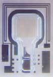
Future developments include integrated metal deposition thermistors and a heater that can provide feedback and maintain constant temperature with reduced thermal transient effects and cost (see Photo). Such a device would allow greater control and efficiency than separate temperature sensors and thermo-electric coolers.
Electronically tunable free-space subwavelength grating filters have been demonstrated in recent years that use liquid crystal to change the refractive index adjacent to a subwavelength grating, resulting in reflection of a tuned wavelength. A detector can be integrated on the wafer level to make the tunable filter into an optical chip for optical-channel monitoring applications. In another derivation, the reflected voltage-tuned beam could be a means to tune or stabilize a laser diode over wavelength or temperature. Precise changes to the pattern of nano-optic elements can be modeled to produce a wide range of different filter shapes to meet different application requirements.
The use of precise photo-mask-based thin-film deposition should lead to additional future optical-chip developments. A select combination of materials can produce a robust metal or ceramic gasket to bond the glass substrates and form a hermetic containment perimeter for the liquid crystal. The result is a better-controlled LC cavity thickness, greatly improved repeatability and aging characteristics, plus the elimination of epoxy off-gassing concerns. The width of the metal gasket can be much thinner without sacrificing yield, quality, or reliability under extreme conditions, enabling future optical chips to be smaller in size with larger active apertures.
Ben Standish is product marketing manager at SpectraSwitch (Santa Rosa, CA).


