APD or FEC in the ONT? That is the question-or, at least if not the question, it does weigh on the minds of many GPON system vendors.
Receivers that implement avalanche photodiodes (APDs) can easily meet the sensitivity requirements expected at the GPON optical network terminal (ONT), but at a high cost. APDs are expensive, require high-voltage biasing, and need to be temperature compensated. FEC adds some cost and complexity to implement the encoding and decoding but is generally believed to be much less expensive than an APD. However, some design challenges and consequently increased complexity and cost are often overlooked when designing a GPON-compatible FEC receiver.
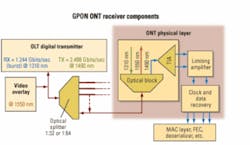
This article describes briefly how FEC works and then illustrates the impact of jitter on a receiver’s sensitivity when using FEC. Actual test data show the expected performance when using two different types of receiver circuits with FEC. The data will highlight important issues that designers should consider when selecting the ONT receiver components (Figure 1) of a GPON system that uses FEC.
FEC is a technique for improving the bit-error-ratio (BER) performance of a digital communication link by encoding the transmitted bits in a manner such that, after the bits have been received, bit errors can be detected and corrected. This generally involves adding extra “redundancy bits” to the data stream using a predefined coding algorithm that is known by the receiver. After the data and redundancy bits have been received (at the “forward” end of the link), the algorithm can be reversed to recover the original data.
As a simplistic illustration, we can consider transmitting a three-bit “code word” for every data bit; e.g., for each “0” in the data, we could transmit 010, and for each “1,” we could transmit 101. If the received code word is anything other than 010 or 101, we know there is an error, and assuming that a single bit error is much more likely than multiple errors, we can easily correct the error. For example, if we receive 000, 110, or 011, the correct code word was most likely 010. The disadvantage of this scheme is that we have to transmit three times as many bits, but the tradeoff is that we can correct all single-bit errors at the forward end of the link.
Many different FEC codes exist and others are in development. Improved codes strive for increased efficiency (less overhead from redundancy bits) while providing the ability to correct more errors. This latter aspect is called “coding gain”; it refers to the increase in transmitted power (or receiver sensitivity) that would be necessary to realize the same improvement in BER as the FEC code provides.While the intricate details of the many coding schemes are outside the scope of this article, there is one general FEC coding issue that is a key point for our discussion: FEC codes tend to be less effective with bursts of errors than with isolated errors that are randomly distributed in the data. Referring to our previous simplistic illustration, assume we transmit the two code words 010 and 101 and that in the process two bits are received in error. If the two errors are spread such that one occurs in each code word, we can easily correct the errors in the received data. But if both errors occur in the same code word, the errors will not be corrected properly. Again, the key issue is that error bursts (as opposed to distributed errors) can significantly degrade the effectiveness of FEC codes.
A common argument is that the probability of error bursts is so small that their effects can be largely ignored. This argument is based on the assumption that each bit has an equal probability of error (for example, 10-9) and thus the probability of having two adjacent bit errors is the square of the probability of a single error (e.g., 10-9 × 10-9 = 10-18) and so forth, so that it is extremely unlikely that multiple adjacent bit errors will occur. This brings up a pair of interesting questions: How valid is the underlying assumption that bursts of errors are extremely unlikely, and are there conditions in which bursts of errors are actually more likely to occur? The answers to these questions have large implications for the design of systems that rely on FEC coding gain.
Two of the most common causes of bit errors are additive white Gaussian noise (AWGN) that occurs in the amplitude of the signal and timing variations between the data and the recovered clock signal that are referred to as jitter.1 Amplitude noise due to AWGN is random in nature and, as shown in most digital communications textbooks, the resulting bit errors occur at correspondingly random times with a probability proportional to the signal-to-noise ratio.2 Jitter, on the other hand, can result from random or deterministic causes. It is the reduction of FEC coding gain due to the effects of jitter that is of primary interest to this article.Jitter is commonly divided into two subcategories: random jitter and deterministic jitter. The most common cause of random jitter is the conversion of amplitude noise to timing noise that occurs as the signal crosses the threshold between a “0” and a “1” at the input to a limiting amplifier (LA).3 Two of the most common types of deterministic jitter are pattern-dependent jitter (also called intersymbol interference, or ISI) and pulsewidth distortion (PWD). ISI occurs when the system bandwidth is not matched to the signal bandwidth; PWD is generated as the transimpedance amplifier (TIA) output becomes small in relation to the sensitivity of the LA. It is very important to note that jitter at the output of an LA generally increases rapidly as the input signal is reduced to near the minimum specified level (sensitivity).
Now let us compare two receiver scenarios, each using a TIA followed by an LA. In both scenarios we will assume the overall gain due to the combination of the TIA and LA is the same. In the first scenario, the TIA gain is higher and the LA gain is lower. Conversely, for the second scenario, the TIA gain is lower and the LA gain is higher. We will consider what happens in each scenario as the input power to the TIA is reduced to near the sensitivity level of the receiver.
In the first case, due to the high gain of the TIA, its output signal never drops to the sensitivity of the LA and therefore the sensitivity of the overall receiver is mostly determined by the input-referred noise of the TIA. In the second case, the TIA output signal does drop to near the sensitivity of the LA; therefore, the sensitivity of the overall receiver is significantly affected by the input referred noise of the LA, as well as the increased jitter generated at the output of the LA. The important point to understand is that it is possible to have the same overall receiver sensitivity for either scenario, even though the mix of amplitude noise and jitter at the output of the LA could be significantly different.
In a typical digital communications receiver, the LA is followed by a clock and data recovery (CDR) circuit. The CDR uses a phase-locked loop (PLL) to generate a clock signal that is synchronized with the incoming data signal. A key specification for the CDR is its jitter tolerance, which is defined as the amount of jitter at the input to the CDR that can be tolerated without causing an increase in bit errors that exceeds a specified threshold. Depending on the architecture of the CDR (which usually correlates with its complexity and price), it may have improved jitter tolerance. Also, some CDRs tolerate random jitter better than deterministic jitter and vice versa.By definition, when the jitter at the input of the CDR begins to approach the specified jitter tolerance, the number of bit errors will increase. An important question in relation to the use of FEC coding is how the bit errors caused by the jitter at the CDR are distributed. Will they tend to occur at random intervals or in bursts? The exact answer depends on a number of factors, including the architecture of the CDR, but in general, the bit errors that result from jitter at the CDR are caused by brief faults in synchronization between the data and the recovered clock that many times result in bursts of errors. As noted above, the mix of amplitude noise and jitter can be altered significantly by the relationship between the gain of the TIA and the gain of the LA, which in turn affects the performance of the CDR and potentially the distribution of the bit errors. As we will show by actual measurements, this can have a profound effect on the FEC coding gain.
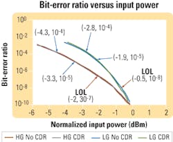
To illustrate the effects of jitter and burst errors in a multigigabit FEC digital receiver, various parameters of two receiver circuits were measured with and without a CDR attached. The first one is a conventional 2.5-Gbit/sec receiver implemented with a PIN diode, a low-gain TIA, and an LA. The second receiver uses a higher-gain, but noisier, TIA. The BER versus input power normalized to the sensitivity level (BER = 10-10) for the two receivers is shown in Figure 2. Assuming that the FEC can compensate for a BER of 10-5 to 10-4, we would expect that the low-gain (LG) receiver with FEC would have a coding gain of about 1.9 to 2.8 dB and that the high-gain (HG) receiver would have a coding gain of approximately 3.3 to 4.3 dB.
The BER with a conventional low-cost CDR attached to each receiver’s output is also shown in Figure 2. Using this as the only reference, we would conclude that approximately the same levels of FEC coding gain (1.9 to 2.8 dB and 3.3 to 4.3 dB for the LG and HG receiver, respectively) would be obtained with the CDR attached. However, as we will show, the actual FEC coding gain obtained with these examples is much lower due to the jitter characteristics of the receivers.
With the LG receiver, the loss-of-lock (LOL) output of the CDR starts to chatter (toggle based on deterministic and random input jitter affects) at a BER of 10-8, which is approximately 0.5 dB below the typical sensitivity level (Figure 2). When the CDR is combined with the HG receiver, the LOL first starts to chatter at about 2 dB below sensitivity. A chatter of LOL does not necessarily indicate errors or bursts of errors, but it gives us a warning that the jitter at the input of the CDR is at or near the maximum jitter tolerance and that an in-depth investigation into the error statistics should be performed.
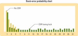
Looking at the burst-error probability on a bit-error analyzer for the same two receivers does show that long bursts (>20 bits) of errors are occasionally occurring at the LOL points shown in Figure 2. Figure 3 is a graph representative of the burst-error probability of the HG receiver with the CDR (green bars) and without the CDR (gold bars) at an error ratio of approximately 10-5. With no CDR, the burst-error distribution is as you would expect for errors that are caused by random events. With the CDR attached, the errors extend to bursts greater than 30 consecutive bits and would result in a significant reduction of the coding gain. With burst-type errors like these, the FEC coding gain at the CDR output would be approximately 0.5 dB for the LG receiver and about 2 dB for the HG receiver.
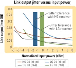
We can gain additional insight into where the LOL chatter, and potentially burst errors, will occur by measuring the jitter characteristics of the link (transmitter → photodiode → TIA → LA) and comparing the results to the rated jitter tolerance of the CDR. The approximate points where the link jitter for the LG and HG receivers exceed the jitter tolerance of the same CDR as in Figure 2 are highlighted in Figure 4. These points correspond to the LOL chatter locations shown in Figure 2.
In Figure 4, we see that the LG receiver has less jitter than the HG receiver at input levels higher than the normalized sensitivity, but the jitter increases rapidly as the input level approaches and goes below the sensitivity point. This is primarily due to the LA sensitivity being large in comparison to the output signal from the TIA. In other words, the gain of the TIA is too low given the minimum input level of the LA used.
The HG receiver has more jitter at input levels above sensitivity; however, it provides an output with less jitter at levels below sensitivity. In this case, the signal at the input of the LA is large in comparison with the LA sensitivity. The LG receiver has a respectable -25-dBm sensitivity at 2.488 Gbits/sec, but with target sensitivity levels of -27 to -28 dBm minimum, the LG receiver is unsuitable given that a maximum of 2.8-dB coding gain is possible even when using an ideal CDR. With an FEC coding gain of 2 dB, the HG receiver operation would be very marginal with a conventional low-cost CDR.Assuming the transmitter jitter has been reduced as much as possible, we see by these examples that one or both of the following component selections should be used when implementing FEC in a GPON system.
Select a high-performance TIA. Selection of the proper TIA is critical for a successful FEC implementation. Assuming a conventional multigigabit LA (2- to 4-mV sensitivity) is used, the TIA should be low-noise (<≈ 250 nA), have a high gain (>≈ 7 kΩ), and have sufficient bandwidth (about 2 GHz). The TIA/LA pair should have a BER of 10-10 at input levels of -27 dBm or lower and have sufficient gain to provide a large signal, compared to the LA sensitivity, at input levels 2 to 3 dB lower than the 10-10 BER input level. Assuming the typical sensitivity of the pair is -27 to -28 dBm, having an FEC coding gain of about 3 to 4 dB should provide sufficient margin to temperature and part-to-part variation while meeting GPON requirements. Unfortunately, TIAs with this level of performance at multigigabit rates will often be more expensive due to the IC processes needed to design them.
Select a CDR with an external reference clock. We can also improve the FEC coding gain by using a CDR with an increased jitter tolerance. While the jitter tolerance of conventional CDRs can be quite good, a CDR with an external reference clock will generally have higher jitter tolerance. Since the OLT contains the main system clock, the CDR must be chosen carefully so that the reference clock will only steer the clock recovery to the OLT frequency while still providing a high jitter tolerance. The main drawback of this implementation is the cost involved with reference clocks and/or the selection of a low-cost CDR with sufficient jitter tolerance.
As we have discussed, GPON systems necessitate very low sensitivity levels for the downstream digital data. Forward error correction can be used to meet the link budgets in these systems, but designing an FEC receiver with adequate sensitivity and coding gain requires high-performance receiver components that may increase the system cost and complexity beyond what is initially expected.Justin Redd, PhD, is strategic applications manager and Craig Lyon is strategic applications engineer at Maxim Integrated Products (Sunnyvale, CA; www.maxim-ic.com).
1. Maxim Integrated Products application note HFAN-4.0.4, “Jitter in Digital Communication Systems, Part 2,” http://pdfserv.maxim-ic.com/en/an/6hfan404.pdf.
2. B. Sklar, Digital Communications: Fundamentals and Applications, Englewood Cliffs, New Jersey: Prentice Hall, pp. 733-743, 1988.
3. J. Redd, “Synch and Clock Recovery-An Analog Guru Looks at Jitter,” Electronic Engineering Times, Planet Analog Section, Issue 1181, Aug. 27, 2001.


