Advances in semiconductor technology and collaboration between systems developers and silicon providers will drive the provisioning of new equipment for Internet-protocol networks.
Achim Hill
Conexant Systems Inc.
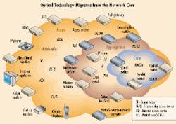
Figure 1. Optical networks increasingly depend on a complex foundation of semiconductor electronics.
The massive evolution of the Internet infrastructure is here to stay, and the world is adopting optical technology at a tremendous rate. Semiconductor industry economics and the continuing evolution of semiconductor technology are helping to fuel this growth, as the cost per bit in chip implementations continues to drive network equipment costs down. At the same time, this unprecedented Internet infrastructure upgrade creates different requirements for semiconductor technology.
Figure 2. A fragmented and evolving network infrastructure requires a complex range of semiconductor solutions.
The first generation of optical transmission equipment moved light across fiber-optic strands in long-haul networks. Later generations of equipment used dense wavelength-division multiplexing (DWDM) to move more waves of light across the fiber infrastructure. This technology has evolved quickly, progressing from DS-0/DS-1/DS-3 to OC-3/OC-12/OC-48 and beyond, as bandwidth needs have increased and carriers have demanded higher-capacity solutions.
But the emergence of wavelength-based networks does not preclude the need for Synchronous Optical Network (SONET) technology. SONET will serve as a service interface to the optical network and coexist with other service interfaces such as Gigabit Ethernet and Fibre Channel.
Meeting the performance challenges imposed by the evolution of the Internet infrastructure requires innovation on multiple levels beyond the simple roadmap outlined by Moore's Law. The development trajectories of DRAMs and microprocessors have been extremely linear and predictable. But that does not necessarily hold for communications integrated circuits (ICs), as the ever-growing need for bandwidth and resulting challenges go well beyond Moore's Law. These challenges include not only integration, but also advanced packaging designs, specialty process solutions, simplified protocol design, and system-architecture innovations. In turn, these opportunities require a new kind of design process-a collaborative design environment that's "vertically integrated" with the customer.
Advances in packaging design enable semiconductor manufacturers to improve costs while reducing product cycle times. Also, when semiconductor suppliers can leverage multiple process technologies such as gallium arsenide (GaAs) and silicon germanium (SiGe) in a single device, there are tremendous opportunities to reduce development cycles. For instance, using multichip module (MCM) technology, one function can be designed in GaAs and another in SiGe bipolar complementary metal-oxide semiconductor (BiCMOS). In addition, MCMs allow manufacturers to "mix and match" intellectual property, integrating complex systems into one MCM without having to design the technology into a single chip.
New MCM technologies, called radio-frequency (RF) micromodules, are emerging. RF micromodules enable both active and passive components like resistors, capacitors, and inductors to be integrated into a single module. That means components, which once went on boards, can now go on-chip.
An excellent example of the integration opportunities possible using the latest packaging technologies is integrating a crosspoint switch for fiber-optic communications systems with a baseband controller into an MCM package, rather than waiting for the two functions to be integrated on-chip. This way, the baseband and digital controller could be implemented in a lower-cost 0.18-micron CMOS process, and the crosspoint switch, which has extensive logic requirements, could be designed in 0.35-micron BiCMOS.
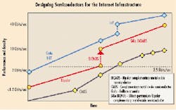
A variety of process technologies are now available for designing semiconductors for the Internet infrastructure (see Figure 3). CMOS is the lowest-cost solution and has the highest integration level. Semiconductors for OC-3 and OC-12 are currently designed in CMOS, and OC-48 and OC-192 are migrating to a silicon bipolar junction transistor (BJT) or SiGe heterojunction bipolar transistor (HBT). In terms of integration, SiGe is an ideal choice, since it's widely available and cost-effective. GaAs is ideal for niche applications requiring high switching speeds such as long-haul drivers.Figure 3. Specialty process technologies are emerging for higher performance and greater density.
The challenge today is developing solutions for 10 Gbits/sec and greater data rates. A new type of compound semiconductor solution, such as indium phosphide (InP), is the primary process in use for managing the interfaces in the 10-Gbit/sec and 40-Gbit/sec optical Internet infrastructure. InGaP excels at handling high-data-rate interfaces. Meanwhile, alternative specialty technologies like SiGe offer a silicon-based path to satisfy the need for high-speed devices for the 10-Gbit/sec market and tomorrow's 40-Gbit/sec requirements.
These technologies allow designers to create lower-power solutions that integrate more of the framers and other logic on-board. SONET products are the drivers for the SiGe BiCMOS and process and 0.18-micron CMOS technology for framers.
In addition to employing new process and packaging technologies, moving beyond the traditional "horizontal" design process is critical to designing next-generation products for the networks of the future. Until recently, the customer would traditionally complete a product design and then solicit involvement from the chip manufacturer. ICs were designed to a specification provided by the manufacturer, rather than conceptualized from a system point of view. In this scenario, design cycles extended to as much as 18 months.
The new model for semiconductor design drives significantly faster design cycles than the relationships of the past. The new model is a "concurrent everything" relationship that begins at the conceptual stage. Both the customer and the semiconductor provider assign collaborative design teams at the onset, and architect the system at the same time the chip is being designed and the process technology is being selected. This type of partnership optimizes product design for both the semiconductor vendor and the network equipment provider and cuts design cycles to as little as five months.
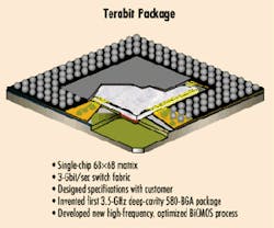
A recent introduction of a 68x68 crosspoint switch for optical networks illustrates the evolution of semiconductor technology and the benefits of a vertically integrated design process (see Figure 4). The semiconductor provider collaborated with its lead customer throughout the system design process to create a switch that provides terabit throughput capabilities, superior electrical performance, and a cost-effective, power-efficient package for large crosspoint-switch configurations.Figure 4. The specification for this single-chip 68x68 matrix was designed in collaboration with the manufacturer's lead customer.
Today's digital crosspoint switching matrix is the most common architecture for handling terabits of Internet traffic and other high-volume communications requirements. To achieve a full terabit of throughput in a single package, another customer worked with the same silicon provider in the invention of the industry's first 3.5-GHz deep-cavity 580-ball-grid-array (BGA) package. It contains 68 differential input lines, at 3 GHz apiece, with additional control lines that bring the total throughput to almost a full terabit. This package was achieved using a new high-frequency optimized BiCMOS process.
By involving the semiconductor provider in the system design process, the right tradeoffs could be made in terms of the functionality of the crosspoint switch and what was required to build the Internet backbone equipment. The requirements of the optical equipment established the requirements for the chip solution, rather than designing the chip from an independently generated specification. Design, packaging, and device technology were developed concurrently, resulting in a completely optimized system design. The packaging could accommodate specific requirements, and the process technology was
customized in a 0.35-micron BiCMOS pro cess, which en abled the industry's highest switch ing density on a single device. This process technology was originally used for wireless applications and customized by changing the interconnect scheme for networking applications.
Working together, systems manufacturers and semiconductor pro viders can meet the performance challenge presented by the Internet infrastructure.
The challenge ahead involves continuing to break the bottleneck of traditional communications system design and foster fast-track innovation. Creating specialty process technologies, advanced packaging techniques, and collaborative relationships between suppliers and customers are key to overcoming the many hurdles and challenges of the new Internet economy.
Achim Hill is vice president and business director for the Integrated Circuits for Optical Networks (ICON) group within Conexant's Network Access Div. (Newport Beach, CA).


