Re-mapping still requires OEO conversion to 'touch bits' for wavelength processing in today's metro and long-haul networks.
KRZYSZTOF INIEWSKI, PMC-SierraWhile the need for electronic components in access networks, LANs, or SANs is obvious, the case for metro and long-haul networks requires closer examination. In the last two years, there have been many attempts to transfer the core of the broadband network entirely to optical. Even so, optical-electrical-optical (OEO) conversion is required in core optical networks and will still be required for years to come, despite the impressive advances in the photonics industry.
The dilemma and the need
Consider an imaginary network of 80-wavelength DWDM traffic between New York City and San Francisco, routed through Denver. Furthermore, assume that wavelengths numbered 1-20 and 60-80 are actually reserved for this traffic. A similar connection from Atlanta to San Francisco, also through Denver, is to be set up with dedicated wavelengths 15-25 and 40-50. Now, the Denver-to-San Francisco connection has a problem: Wavelengths 15-20 are double-booked, even though there is still spare capacity in the fiber and a number of free lambdas not assigned.
To solve this problem, the Denver facility has to re-map wavelengths 15-20 to some free lambdas, say wavelengths 30-35. Unfortunately, there is no optical device currently on the market that can perform this conversion in the optical domain, although some interesting optical devices are being explored in research labs.1
The only way to perform the re-mapping is to convert the optical signals into electrical ones, optionally process them, and convert them back to the optical domain using different wavelengths. A side benefit of the OEO conversion is 3R (regeneration, reshaping, retiming), which is not possible in the optical domain.2
OEO conversion today
So how is the OEO conversion done today? For regeneration applications (see Figure 1), the optical signal is received by a photodiode (PD) whose resulting small output electrical current is converted to a voltage-domain signal by a transimpedance amplifier (TIA) and sent to a clock recovery and synthesis unit (CRSU). The CRSU recovers the clock information from the data stream using phase-locked-loop (PLL) or digital phase-picker circuitry, demultiplexes the signal down to lower speeds, and sends it to a forward error correction (FEC) device.
The data is then sent to a laser driver (LD) that modulates the laser. For network flexibility, the ideal laser should be a tunable device that can generate optical signals in a certain optical bandwidth, not just one particular wavelength. In practice, at high frequencies, it is very difficult to modulate the laser directly due to the chirp effect, which prevents clean modulation. As a result, external modulators, usually based on lithium niobate, are used.
The laser, LD, PD, and TIA in Figure 1 together create an optical data link (ODL) module. The CRSU multiplexer/demultiplexer may be part of the ODL module, or it may be placed on the printed circuit board (PCB). Both variants are available commercially. If the CRSU has difficulty resolving the very small signals received from the TIA, then an extra component such as a limiting amplifier or post-amplifier may be required. Also, as mentioned earlier, an external laser modulator is required to handle high frequencies.
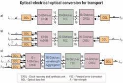
To further illustrate applications of OEO conversion, consider the optical transport equipment that must process optical wavelengths at OC-192, OC-48 (2.5-Gbit/sec), and Gigabit Ethernet (GbE) rates. The equipment will have three different pro cessing cards: an OC-192 SONET/ SDH transponder, a 4 x OC-48 SONET/ SDH muxponder, and a 10 x GbE muxponder (see Figure 2).
The OC-192 transponder card uses the generic configuration of Figure 1, with a 10-Gbit/sec CRSU performing clock recovery and synthesis functions. Typically, the CRSU will demultiplex the 10-Gbit/sec signal into 16-bit-wide parallel signals for easier processing downstream.The 4 x OC-48 SONET/SDH muxponder card is similar, but instead of processing one OC-192 stream, four OC-48 data streams are multiplexed into an OC-192 pipe. This function is performed by a quad OC-48 CRSU device (CRSU-4x2,488). Again, the output from the CRSU-4x2,488 is 16 bits wide.
Finally, the 10 x GbE muxponder card aggregates 10 GbE channels into one OC-192 signal, maximizing bandwidth efficiency through the use of SONET/SDH virtual concatenation. In this case, the 10 x 1-Gbit/sec CRSU performs the clock recovery and synthesis function, although because of the relatively low clock rate (1.25 GHz), this function will likely be integrated with the wavelength aggregator device.
Design challenges
What are the complexities and challenges of building the existing electronic devices in OEO converters? TIAs are the most sensitive to noise. As a result, they have traditionally resisted chip integration and are frequently manufactured in exotic bipolar technologies. Many attempts to design TIAs in CMOS have been made recently, but the performance of the finished devices is still poor. The device is often integrated with an avalanche photodiode.
From a high-speed analog design perspective, the CRSU transceiver is the most demanding device to build. Despite the threat of directly sending IP traffic over DWDM, today's networks are still SONET/SDH-based and will likely remain so for a while due to incumbent local-exchange-carrier dominance.
Therefore, the transceiver needs to be compliant with the rigorous Bellcore SONET/SDH jitter specification. In particular, achieving a 0.1-unit-interval peak-to-peak (UIp-p) of intrinsic jitter, while transmitting the SONET/SDH data stream, imposes harsh requirements on the phase noise characteristics of the synthesizer's PLL. It takes years of analog design experience to build manufacturable and jitter-compliant devices.
The FEC device is the most demanding to build from the algorithmic point of view. The key is to deliver the highest coding gain with the lowest overhead rate. Traditional Reed-Solomon coding-implemented in standards like the G.709 digital wrapper-offers a 6-dB coding gain at 7% overhead, while many proprietary FEC schemes offer a 10-dB gain (or more) at the expense of 25% overhead. For most applications, the market currently demands an 8-dB gain with only 7% overhead. With a fiber loss of 0.2 dB/km, an extra 8 dB of gain provides about 40 km of signal reach, which is important in metro long-reach networks.
Manufacturing processes
In the first generation, core network deployment devices were typically manufactured in an exotic process like gallium arsenide or silicon germanium (SiGe). Since neither process offers integration possibilities and both processes have lower yields than CMOS and are power hungry, they are typically displaced in a second-generation deployment by CMOS parts. Currently, 0.13- micron CMOS processing power is sufficient to design and manufacture OC-192 SONET/SDH-compliant transceivers that consume half the power of their SiGe counterparts.
Going forward to OC-768 (40-Gbit/sec) rates, this deployment scenario will not likely change. In the race to OC-768 performance, however, indium phosphide (InP) seems to be the leader with the highest raw speed power, with SiGe technology trying to catch up. CMOS technology, with a move to 0.1-micron feature sizes and some design innovation brewed at several universities and research labs, is likely to catch up and displace both InP and SiGe later, when the real OC-768 volumes will be needed. In the meantime, the photonics industry is working to improve the performance of components that can work directly with CMOS-based CRSU devices without need for TIAs.
Another trend in the manufacturing process is device miniaturization through integration of a photonic device like a PD receiver with an electronic device like the CRSU transceiver. If both components are manufactured in InP, this integration is possible today. But the problem is photonic devices require very careful alignment to the fiber, resulting in a high cost of packaging and assembly.
Furthermore, the larger photonic-electronic integrated die requires a larger package and PCB area than two less expensive, separate components: one photonic and one electronic. At the moment, homogenous integration, like that used in CMOS, pays off, but heterogeneous integration of photonics with electronics is still not economically feasible. Certainly, a lot of effort and investment are being made to make photonic-electronic integration achievable in the future.
The inherent functional shortcomings of optical devices make it unlikely that the core of the network will become an entirely optical domain. Most important, the lack of an effective method of wavelength conversion, or re-mapping, coupled with the economies of scale and ever-increasing performance of the technology mean that electronic devices will continue to be deployed at 10- and 40-Gbit/sec rates.
Some additional limitations of all-optical devices, such as the lack of optical storage and the inability to analyze the content of the optical signal, further dictate the need for electronic devices where these functions currently exist or can be realized. Even as future network rates increase, the need for OEO conversion will likely continue to address functions that are not optically feasible.
Dr. Krzysztof (Kris) Iniewski is manager of strategic marketing at PMC-Sierra's optical-networking division (Burnaby, British Columbia). He can be reached via the company's Website, www.pmc-sierra.com.
References
- J.P. Laude, DWDM fundamentals, components, and applications, Artech House, 2002.
- R. Ramaswami and K. Sivarajan, Optical Networks: A practical perspective, Academic Press, 1998.


