Moving closer to 'systems on a chip,' there are cost advantages for feature integration.
JONATHAN WALDERN, DigiLensOver the last year, the market for optical DWDM equipment may be best characterized as experiencing digestive problems. However, the growth of bandwidth services and data consumption continues unabated. Cost, performance, and flexibility are the primary drivers for optical-network-system deployment and upgrades, where reduced inventory, installation, upgrades, power consumption, and service costs compose the true cost of ownership for operators.
Despite the highly compelling futuristic applications that were sold to all during the Internet bubble, the bandwidth industry will remain on idle-unless fundamental change occurs in optical-component and optical-system cost and performance. Carriers require dramatic improvements if they are to provide a compelling broadband service to consumers and businesses and make the bubble dream come true.
Network systems are made from components, modules, and subsystems. Current "discrete" optical components have evolved in step with demand since the early DWDM long-haul transmission systems were first deployed. Today, these components are sophisticated variations of their predecessors and beautifully made by talented individuals.
To broadly deploy the optical layer into metro and access markets, however, system specifications call for electrically reconfigurable agile modules containing sophisticated multiport functionality. For monitoring routing or conditioning DWDM wavelengths, existing handmade components are a less than ideal platform. A new generation of technology is now driving highly integrated solutions, echoing the electronics industry's transition from transistors and capacitors to ICs.Integrating into a single device the multiple functionality usually found in discrete components is undoubtedly the best way to reduce costs through avoidance of optical interconnects, shared electronics, power supplies, packaging, and inventory control. But in the near term, the largest savings come from packaging. Today, 50-80% of the cost of an optical component can be attributed to its packaging and associated yield.
Notwithstanding increased packaging automation of current generation components, if multiple component functionality can be integrated monolithically, significant cost savings can be made. But when considering the tradeoffs pertaining to the cost of fabrication, the performance and yield of any functional element makes it unclear exactly what integration approach offers the best solution.
Defining integration
Three terms are commonly used today to describe various phases of integration. "Discrete" refers to the single components with an individual function. "Hybrid" refers to an assembly of different devices made using various materials or technologies but sharing a common, often hermetically sealed, package. Finally, "monolithic" is used to describe a single component that is capable of performing multiple optical functions either in series or parallel.
Interestingly enough, the word monolith comes from the Greek word "monolithos," literally translated as "single stone." The derivation "monolithic," according to the American Heritage Dictionary, means "massive, solid, and uniform: the monolithic proportions of Stalinist architecture." How, as an industry, we have come to adopt this term to describe the zenith of optical integration remains a mystery.
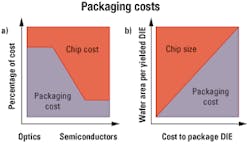
Currently, packaging represents the dominant share of component cost. Figure 1a contrasts the relative cost of packaging associated with optical components today, compared with the semiconductor industry where packaging has evolved to represent a small fraction of the component cost.
Typically in both optical components and semiconductors, packaging costs will scale proportionally with the volume of the packaged product. As shown in Figure 1b, it logically follows that the smaller the component, the lower the packaged cost will be. In addition, smaller components take up less subsystem real estate, which allows smaller, lower-cost system installations.
That is where planar waveguides clearly become valuable, lending the ability to guide, interconnect, attenuate, and switch lightpaths without leaving the chip. They offer all the benefits of automated manufacturing learned from years of experience in the semiconductor industry.
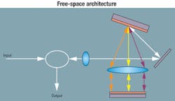
Free-space integrationToday, most optical integration typically involves linking together different discrete components, using either free-space coupling, fiber interconnects, or direct bonding to perform a composite task within a shared package. An example of this type of integration with free-space components would be the use of micro-electromechanical systems (MEMS) arrays with a dispersive grating (see Figure 2).The light follows a relatively complex optical path through various lenses before being dispersed or demultiplexed by the grating and projected onto an array of mechanical mirrors. Light is then reflected back off the grating according to the tilt of the mirrors before passing back through the optical chain and out of the device (often via a circulator). While significant advances have been made in MEMS devices, the alignment tolerances, thermal expansion considerations, and isolation from vibration inevitably add to the packaging cost.
Steps to planar integration
Another approach is to connect various planar-waveguide devices, each with its own optical function, together inside a single hermetic package. These waveguides are connected using either fiber interconnects or by bonding the waveguides, core to core, to create a "seamless" optical path.
Examples include the Vmux devices offered by several planar-waveguide vendors over the last few years and more recently the dynamic gain equalizers and channel equalizers that integrate separate waveguides for the arrayed-waveguide-grating (AWG) demultiplexer, variable-optical-attenuator (VOA) array, and AWG multiplexer together with shared packaging and electronics to complete the "subsystem." While the price points of these devices are arguably lower than achieving the same functionality using discrete components, they are still a long way from reaching the cost and performance required.
In any integration scheme-free-space or planar-waveguide-selective control of individual wavelengths will for the most part require demultiplexing of the signal into bands or channels before processing and recombining via an AWG or thin-film-filter multiplexer. Unfortunately, most demultiplexing/multiplexing schemes largely necessitate discrete-component assembly, which negates many of the cost benefits of hybrid planar integration.
The majority of these hybrids use thermo-optic switching to route signals. These discrete planar waveguides must be coupled together physically and optically with expensive packaging and high power consumption due to the thermo-optic elements-all of which conspire to increase subsystem cost.
Additionally, thermal expansion coefficients of these discrete subcomponents must be carefully managed to avoid potentially disastrous stress-induced failures. Advocates of this method of integration also concede that achieving acceptable coupling efficiency between waveguides still requires submicron alignment tolerances. Misalignments greater than a couple of 10ths of a micron for waveguide components with core dimensions on the order of 5 microns that are coupled to singlemode fibers with core dimensions on the order of 10 microns will result in significant attenuation of coupled power.
Thermal crosstalk can also be a problem, imposing strict limitations on how closely elements can be placed on the waveguide and dramatically reducing the number of features per unit area that can be put onto the chip. The very physical phenomenon that enables thermo-optic devices is also its Achilles heel.
Integration of separate planar waveguides in this manner is a step in the right direction, certainly compared to the labor-intensive free-space approach, and saves significant packaging costs over the discrete alternatives. But the size, power, and thermal constraints make them less attractive solutions when compared to the fully integrated single-chip alternative.
Going forward, these types of free-space and planar integration methods will likely be reserved for isolated instances where a comparable solution cannot be achieved through single-chip integration techniques or where the volumes are so low that the manufacturing setup costs cannot be justified.
"Subsystem on a chip"
The goal is undeniably to achieve a level of optical integration on a chip that begins to parallel the cost efficiencies found in the world of integrated electronics. In this context, we will assume the "chip" refers to a single wafer-derived component that can be processed using the same automated manufacturing techniques used in the semiconductor industry. The critical drivers here are cost, size, and on-chip interconnection that leads to minimal packaging and high yield.
As described earlier, the state-of-the-art in terms of photonic components has been analogous to a collection of resistors, capacitors, transistors, and switches assembled together by hand into photonic assemblies or subsystems. Some argue that is where the comparisons between electronic and photonic ICs stop-the major issue being that, unlike silicon used in semiconductors, there is no single optically transparent material that can perform all the necessary telecommunications functions. That is almost certainly true for the near future. But compared to the current state-of-the-art in optical components, any scalable material platform that allows the monolithic integration of a subset of functions, including filtering, tuning, attenuation, switching, and blocking, will provide dramatic improvements in cost and performance.
DWDM optical components that leverage the same basic "on-chip" building blocks to perform these different compound functions such as dynamic spectral or gain equalization, optical add/drop multiplexing, or variable optical attenuation will benefit disproportionately in manufacturing efficiencies as volumes increase. In the next few years, it is unlikely that any single platform technology or material system will ever achieve the complete set of active and passive requirements needed for optical systems, but several are emerging as contenders.
Theoretically, indium phosphide (InP)-based solutions offer the potential of mixed active and passive functional integration. However, the cost of development of a dedicated process that can yield an integrated multifunctional component for use in broadband DWDM applications is currently not economically possible.
Lasers, detectors, passive structures such as attenuators, switches, and tuning, including control electronics, all require different processing steps that are mostly incompatible. Yield coefficients currently limit cost-effective integration to only one or two features. It is argued that successful integration platforms may come from developing a unified manufacturing process that can integrate a set of "proximal" functionality like filters, VOAs, monitors, switches, and add/drops, while adding active devices such as lasers and detectors to the chip afterward as a hybrid device. That maximizes product yield and lowers cost.
Carriers will continue to demand significant improvements in optical-system cost, performance, and agility. The improvements in free-space integration efforts and power-hungry thermo-optic waveguides are unlikely to fulfill future demands for high feature modules required in next-generation designs.
A manageable approach to integration, producing highly scalable low-cost multifunctional photonic chips is the key. To fully exploit the opportunities of integration, manufacturers must look beyond just solid-state versions of existing discrete devices. Rather, they must innovate new highly integrated devices with an order of magnitude cost and performance improvement.
Multiplexer/demultiplexer filters, attenuators, switches, monitors, and amplifiers must be incorporated into the same miniature packaged device toward the "system on a chip" capabilities offered by the electronic counterpart. Integrated technology platforms will participate in this next-generation race to agile optical components. That in turn will contribute to disrupting the current cost and performance impasse, enabling proliferation of the optical layer in terrestrial networks.
Jonathan Waldern is founder and CEO of DigiLens Inc. (Sunnyvale, CA). He can be reached via the company's Website, www.digilens.com.
References
- "Wavechip Monolithically Integrated Tunable Photonic Integrated Circuits for Next Generation DWDM Applications," DigiLens Inc., May 2002.
- R. Rubenstein, "The Need to Reduce Component Cost Drives Integration," RHK Inc., March 2002.
- J. Mills, "Photonic integration combats network complexity," FibreSystems Europe, May 2002.
- B. Shine, et al., "Hybrid integration optimizes PLC module design," WDM Solutions, November 2001.


