Startup makes nanophotonics device with DUV photolithography
by Meghan Fuller
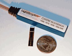
Though president and chief executive officer Thomas Mossberg calls the half-dozen people who compose startup LightSmyth Technologies (www.LightSmyth.com) “a conservative bunch,” those same people are responsible for leveraging deep ultraviolet (DUV) photolithography, borrowed from the electronics world, to develop nanometer-scale optical components. The first such component, a four-channel CWDM multiplexer/demultiplexer, is based on a device that LightSmyth calls a holographic Bragg reflector.
The physical device is similar to an arrayed waveguide (AWG), says Mossberg, in that it comprises three layers of glass on a silicon substrate, and the light is confined to the center layer. However, LightSmyth uses DUV photolithography to etch a very fine pattern of lines into the surface of one of those layers, and that pattern serves as a filter, reflecting only light within a certain bandwidth.
For this reason, the LightSmyth device functions more like a thin-film filter, even though it is made in the integrated format of an AWG. “When light is traveling through the waveguide, it’s hitting the lines that we have patterned and etched using lithographic tools and from each interface, there’s a reflection,” explains Mossberg. “The sum of all the reflections from those interfaces produces the output signal.” The same is true for a thin-film filter, which is made from multiple thin-film layers, the exact spacing and refractive indices of which allow the filter to select specific wavelengths.
While the physics of the thin-film filter and the holographic Bragg reflector may be the same, says Mossberg, the format is radically different. The LightSmyth device is monolithically integrated whereas thin-film filters are intrinsically discrete devices. For this reason, he says you could describe the holographic Bragg reflector as “a fully integrated thin-film filter-and it’s not just one filter,” he notes. “It can be a whole array of them integrated on the same chip.”LightSmyth’s success hinges on its use of DUV photolithographic patterning tools, which enable quarter-micron and finer resolution. AWGs, by contrast, typically cannot be made much finer than several microns. LightSmyth’s holographic Bragg reflectors are smaller by a factor of 10.
Moreover, he says, holographic Bragg reflectors function via multipath interference-similar to thin-film filters-and thus provide flexible passband control without adversely affecting the insertion loss. “The basic problem with the AWG is that the outputs to go back into the fibers are singlemode, and they only accept a very specific angular range,” Mossberg explains. “An AWG sends different colors in different angles, but singlemode receivers don’t like that.” Like the thin-film filter, the holographic Bragg reflector sends light back in a single direction. For this reason, he says, “we can make very flat-top, controlled passband filters with no impact on insertion loss.”
LightSmyth Technologies has taken its patented holographic Bragg reflector technology and leveraged it in the development of a singlemode-compatible, four-channel CWDM multiplexer/demultiplexer. The monolithically integrated silica-on-silicon device is athermal and polarization insensitive to 0.2 dB.
According to Mossberg, development of the CWDM multiplexer is complete, and samples are available; several already have been shipped to select customers. However, the company has decided to partner with a larger producer to bring the device to market, and Mossberg reports that the company currently is in discussions with potential production partners.
Looking ahead, Mossberg believes the same device is compatible with direct implementation in indium phosphide (InP). For now, a key obstacle to silicon photonics is the challenge of coupling in and out of the silicon chips, which is complicated by insertion loss and a high refractive index.
LightSmyth Techologies and others, including Luxtera (www.luxtera.com), are hard at work to overcome this and other challenges.
Mossberg says there is “a great deal of connection between those areas of interest, of taking silicon photonics and making it practical by eliminating the problem of coupling in and out of the material.” For his part, he hopes to see momentum build around DUV photolithography, which he cites as “the enabling tool for practical nanophotonics.”

