DWDM networks require precise control of spectral emissions and power levels to achieve tight channel spacing, which in turn requires continuous monitoring and correction of network elements such as transmit laser sources, optical add/drops, and optical amplifiers.
Variable optical attenuators (VOAs) are often used to groom power levels across the DWDM spectrum, minimizing crosstalk and maintaining the desired signal-to-noise ratio. For instance, VOAs can be used in cascade with an EDFA to help equalize the amplifier's non-uniform gain profile versus wavelength, resulting in improved linearity and enhanced control of the overall system. Measurement and control algorithms can be developed in a closed loop fashion to provide quick and accurate dynamic closed loop control. Closed loop control techniques are necessary to ensure repeatability and minimize production calibration and trimming. Logarithmic amplifier front ends aid in conditioning the measurement signal, allowing the use of lower resolution and lower cost signal-processing components.
In digitally controlled VOA (DVOA) applications, input and output optical taps are used to measure the absolute optical power at the input and output ports. The power measurements can then be processed to compute the absorbance of the DVOA for a particular attenuation setting. In a closed loop manner, the input and output power measurements can be used to dynamically control the attenuation, thus maintaining the desired signal level. This mode of operation is called automatic attenuation control (ACC). An alternate mode, automatic power control (APC), is also necessary when the output power of the VOA must remain constant as the input optical power varies. In either mode of operation, the loop is typically implemented in the form of a mixed-signal solution, where a digital microcontroller or DSP processes the analog inputs and drives the appropriate control signal to maintain the desired level of attenuation. In fast control loops, it may be necessary to implement the solution completely in an analog fashion to eliminate the latency associated with a digital control solution.
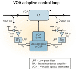
Classic solutions have used linear transimpedance amplifiers (TIAs) and high-resolution signal processing to measure and control the absorbance of the VOA. That seems like an attractive solution because of the low cost of the TIA front end, but the linear nature of the TIA means that floating-point processors must be used to cope with the division and exponentiation processes required to estimate the decibel attenuation across the VOA. An alternative method uses integer-based processing with exhaustive lookup tables generated during production calibration. Both solutions require >14-bit analog-to-digital conversion and moderately high processor speeds to minimize measurement latency due to the processing overhead. The cost advantage in selecting a TIA front end is often lost due to the higher-priced converters and processors needed to acquire the measurement signal and compute the attenuation. Additional cost is incurred if lengthy lookup tables need to be generated during production testing.Figure 1 illustrates the concept applied around an adaptively controlled VOA. The amplified signal is low-pass-filtered to reduce measurement noise. The filtered signal is then digitized and the absorbance of the attenuator is computed.
If linear amplification is used to convert the measured photo currents to proportional voltages, it will be necessary to calculate the ratio of the measured signals. That must be followed by inverse exponentiation and multiplication to compute the VOA's actual absorbance. If the photodiode (PD) responsivities and transimpedance gain of the detector front ends are equal, then the absorbance can be calculated in terms of the output voltages alone. However, backend processing will still be required to compute the decibel value of the ratio.
In reality, the transresistance of each front end will not be equal, requiring additional calibration and correction. To provide acceptable precision in the calculation, the signal needs to be digitized using high-resolution analog-to-digital converters. The design operates in a closed loop manner as long as the input signal is sufficiently large, such that the detected signals are above the noise floor. Variable transresistance may be used to help extend the range of closed loop operation. When the signal falls below the acceptable level for accurate detection, the VOA indicates the lack of signal power and operates in an open loop manner—and is no longer able to guarantee the desired accuracy.
A translinear log-amp is based on the log-linear relationships exhibited in a bipolar junction transistor (BJT). Any BJT exhibits a natural logarithmic relationship between the collector current, IC, and the resultant base-to-emitter voltage, VBE. A single BJT alone makes an impractical log-amp due to the strong temperature dependencies between the transport saturation current, IS, and thermal voltage, kT/q. To make use of the BJT as an accurate logarithmic element, these temperature dependencies must be corrected.
Few analog circuit designers successfully implement discrete designs, utilizing matched transistor pairs and exotic temperature compensation circuitry. Such solutions are difficult to manufacture due to component variability and localized thermal imbalance. Recent advances in monolithic integrated circuit design now allow for the implementation of translinear logarithmic amplifiers that provide wide-dynamic-range signal compression without the temperature dependencies inherent in a discrete implementation. Component mismatch can be better controlled using ratiometric circuit techniques that are more readily designed in an integrated format. Single-chip measurement subsystems are now available, capable of several decades of accurate performance. Such devices provide an output log-voltage of the form:,
where VY is the logarithmic slope, expressed in volts per decade, and IREF is the reference current over which the logarithm is computed.
When considering the incident optical power on a PD, the resulting photo current is directly proportional to the incident optical power in watts. On a decibel scale, the optical power is proportional to the logarithm of the photocurrent scaled by the responsivity of the particular PD. If the reference current is known, the absolute power incident on the PD can be calculated from the VLOG voltage. It is possible to solve for the log-voltage in terms of optical power in decibels:where
That provides a linear-in-decibel transfer function, allowing a simple straight-line equation to describe the relationship of absolute optical power to the output log-voltage. Now simple subtraction and multiplication can be used to assess the decibel optical power without the need to calculate the exponentiation or to use an exhaustive lookup table that would be required if a linear TIA front end was applied.
If the numerator current is derived from the photo current of an input tapped detector, IPD, and the denominator current, IREF, is the resulting photo current after the input signal has passed through an absorptive element such as a VOA, the first equation above can be used to derive the attenuation in terms of the log-voltage:.
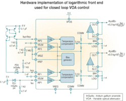
A similar expression could be derived for an optical-amplifier design where it is desirable to compute the gain in decibels across the amplifier. A simple two-point calibration is used to describe the straight-line equation relating the output log-voltage to VOA attenuation setting. In this manner, translinear log-amps provide the capability to measure absolute power, optical absorbance, and gain using a simple linear calculation.The circuit implementation shown in Figure 2 uses a dual translinear logarithmic amplifier, which is capable of using two independent PDs to measure the absolute power on two separate optical supervisory channels. That will allow for absolute measurement of the output optical signal while simultaneously providing a measure of the attenuation. This design utilizes a Wilson current mirror to feed an opposite-polarity replica of the cathode photocurrent of PD2 into channel 2 of the amplifier. Other current mirror implementations would also work, though the modified Wilson mirror provides fairly constant performance over temperature. It is essential to use matched-pair transistors when designing the current mirror to minimize the effects of temperature gradients and beta mismatch. The outputs provide the desired linear-in-decibel transfer functions needed for closed loop analog control. Automatic attenuation and power control can be achieved by comparing the appropriate measurement signal, either attenuation or absolute power, against a desired set point and using the resultant error signal to drive the control signal of the VOA.
Initial prototypes used the dual log-amp to make two independent absolute power measurements, where each PD utilized a single independent channel. That allowed simple differencing circuitry to be applied at the outputs to calculate the attenuation setting, while preserving absolute power accuracy on each channel.
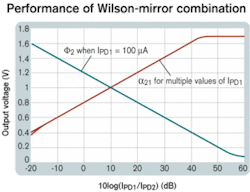
The individual logarithmic slopes of a dual-channel device would be ideally identical. In reality, the channel-to-channel slope mismatch was found to be as high as 5%, resulting in a residual error on the attenuation measurement as the overall power levels changed. Over a five-decade power range, the residual error could be as high as 2.5 dB. In a mixed-signal solution, the residual error could have been predicted and minimized by monitoring the absolute power on one detector and using the appropriate lookup table for error correction.The current mirror solution allows a single channel to be used to measure attenuation while dedicating the second channel to absolute power measurement, thus enabling both AAC and APC with a single measurement IC. This technique eliminates the channel-to-channel mismatch issues that occur when two independent channels are used. Individual channel slope and intercept characteristics can be calibrated independently. The accuracy was verified using multiple calibrated current sources to eliminate any error due to the integral nonlinearity of the VOA. The performance of the circuit is presented in Figure 3. The accuracy is better than 0.1 dB over a five-decade range. The dynamic range is slightly reduced for strong IIN input currents. That is due to the limited available swing of the VLOG pin and can be recovered through careful selection of input and output optical tap-coupling ratios.
Translinear log-amps simplify VOA absorbance measurements by providing a linear-in-decibel relationship between the input photocurrent and resultant output voltage. The division and exponentiation processes required with a linear solution are eliminated when using logarithmic signal processing. There are several methods for using translinear log-amps to provide absorbance and absolute power measurements for AAC and APC control loops. A modified Wilson-current mirror approach is essentially immune to channel-to-channel mismatch and capable of providing more than four decades of measurement and control range.
Eric J. Newman and Matthew Pilotte are applications engineers, Advanced Linear Products, at Analog Devices (Wilmington, MA). They can be reached at [email protected] and [email protected].


