Manufacturing, Packaging & Integration
Nanostructures—structures with one or more dimensions measured in nanometers—produce a broad range of important and often unexpected optical effects. By operating in the subwavelength realm, nanostructure-based optical components, known as subwavelength optical elements (SOEs), can reach and sometimes cross the boundary between classical and quantum optics. The result is a range of effects that surpass those achieved by conventional bulk optical components. These functions include polarization, phase, wavelength, and refractive index filtering or modification. Thus, SOEs offer the potential for a vast improvement in component and subsystem customization, performance, and integration.
To go from research to commercial viability, however, requires cost-effective volume manufacture of SOEs. Given the difficulty component manufacturers face achieving consistent yield and automated production, how can anyone economically manufacture parts with features ranging from 1/100th to 1/10,000th the size of those of current bulk optics?
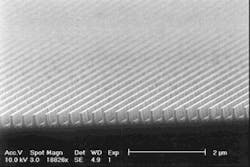
The answer lies in the interplay between SOE design and manufacturing technology known as nano-imprint lithography. SOE physics allows small changes in feature size, shape, or material to produce radically different, desirable optical effects. Nano-imprint lithography can capture each new SOE design and its nanoscale variations accurately, transforming them into wafers ready for manufacture using standard semiconductor manufacturing techniques. Each nano-imprint-produced wafer can yield thousands of high-quality SOE chips (see Photo 1).Most significantly, the interaction between light and gratings at this scale produces none of the high-order diffraction that is characteristic of classical optics. In effect, the property gives component designers all the light to work with. It thus offers enormous flexibility in manipulating the light to produce different effects. That is done by varying the size, shape, and spacing of the grating structure, its materials and the neighboring materials on which it is deposited. In the one-dimensional grating of Photo 2, for example, appropriate selection of size, shape, spacing—or introduction of other variables like deposited metal—will result in an SOE that acts as a polarizer, waveplate, or polarization-dependent filter. Non-grating-based nanopatterns yielding microlens arrays and photodetector arrays have also been demonstrated.
These broad-scale optical functions represent only the beginning of what is possible. Fine-scale variation of optical properties can be introduced in multiple ways, for instance, by rotating a grating pattern 90 degrees and merging it with a similar pattern, thus creating polarization independence. Or dynamic actuation, either thermal or electrical, can be incorporated in the SOE device to allow wavelength tuning, polarization, or refractive index properties.
The cumulative result of this ability to vary suboptical qualities is a dramatic expansion in the range of optical-device customizations. Even for a basic polarizer, the design possibilities include multiple performance levels, selectable narrow or broad wavelength bands, and single or arrayed beam configuration—each achievable by the appropriate nanostructures. Multiply that by the variation in conceivable materials and it's possible to see what is achievable. SOE design flexibility can create thousands of combinations of parameters for something as basic as a periodic grating. Imagine the effect of introducing additional dimensions, changes in shape, variations in period, and multiple layers.
The phenomenal range of designs possible with SOEs has several important implications. One is that systems designers can specify exactly what they need up-front, and subsystems builders can deliver it at a performance and cost appropriate to the task. An infrared application requires a slightly different device than a near-infrared application, as do similar but different applications for long-haul, access, etc. In other words, the constraints of conventional bulk optical-component design need no longer hold optical systems captive.
Another implication is easier volume manufacturing. The relation of function to size, shape, and spacing of the nanostructures decreases the dependence of SOEs on specific materials with specialized manufacturing requirements. For example, designers can select a substrate material but vary the nanostructures to achieve a range of different performances. Use of one material throughout a device in turn can simplify fabrication. It remains, however, relatively easy to add specific materials to fine-tune variations in performance.
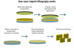
The ability to develop and transfer nanostructure designs to working molds opens the way to volume manufacturing (see Figure). This innovation is key to the SOE manufacturing process and the one protected by the most fundamental intellectual property.SOE component designers begin with simulation tools to determine pattern structure and answer such questions as: Should the gratings appear periodically or non-periodically, be one-dimensional or multidimensional, and have one or multiple layers?
Once the SOE design is specified, the next step is to fabricate a master mold. To accomplish that, various optical lithography techniques, including electron beam lithography and optical holography, may be used to create the nascent nanopatterns. In the holography process, for example, an ultraviolet (UV) laser is used to generate light at around 300 nm, which is split and recombined to generate an interference pattern on the target surface of a pretreated wafer. Widening the angle of the split laser beam and increasing its frequency shorten the periodicity of individual gratings and vice versa. For polarizers, beam splitters, and beam combiners—the first commercially available products manufactured using nano-imprint lithography—the periodicity of individual grating structures is a calculated fraction of the wavelength used in the application.
The pretreated wafer destined to become the master mold is typically a silicon or glass wafer coated with a chosen target layer and, on top, a photosensitive polymer. The polymer layer captures the UV pattern, with those parts of the polymer exposed to light left to be etched out, exposing the target layer below. The next step is to dry etch the target layer and remove the remaining polymer layer.
What remains is a nanopattern transcribed on the hard target layer from the soft, easy-to-write-on polymer. That is the master mold.
The master mold is not used directly in manufacturing, however. Instead, it serves as the fountainhead yielding virtually unlimited clone molds, which will be used in the actual fabrication process.
The process of mold duplication is much the same as for the original mold. The primary difference between the two processes is in the transfer of the pattern to a polymer. Instead of using optical holography, technicians transfer the master mold pattern by imprinting it on a proprietary polymer resist with just enough viscosity to accurately hold the imprint without distortion. After etching, an exact replica of the target layer on either a silicon or glass duplicate of the master mold remains.
The overriding question about such a process is: How, through each of its multiple steps, does the process maintain nanoscale accuracy? The ability to create precise nanostructures on these hard, reusable duplicate surfaces is the key to the commercial viability of SOE production.
To achieve this goal, engineers have developed multiple techniques. At the optical holography stage, for example, they are able to create structures as small as 10 nm and as large as 500 nm with the precision of a few nanometers by varying the laser frequency and adjusting the angle of the split laser beam. In practice, a key to maintaining accuracy is to use a stable optical holography laboratory with all the lasers in semi-permanent alignment plus rigorous process discipline.
Another crucial requirement is to keep the nanostructures consistent in size and shape. This need is apparent since the optical properties are determined by the pattern and shape of the nanostructure. Precisely controlled etching techniques developed through years of experience in SOE fabrication and semiconductor manufacturing play crucial roles. Additionally, uniformity of imprint pressure, temperature, and environmental conditions in the creation of the duplicate molds is important.
Last, but by no means least, device precision is maintained by the subwavelength character of the nanostructures themselves, which counter-intuitively are more forgiving of fabrication variations than if they were larger than lightwaves. That's because the effect on the transmitted light as it interacts with nanostructures is the statistical sum of numerous local interactions between the light and grating. For instance, if a light beam 300 microns in diameter is incident on a two-dimensional grating, where the structure size is roughly 100×100 nm, it illuminates nearly two million nanostructures. Therefore, fabrication variation is overwhelmed by the volume of interactions.
Once the clone molds are prepared, they are used in the standard nano-imprint lithography manufacturing process. The basic steps are very similar to the creation of the master mold, except the holographic process for creating the grating pattern is replaced with an imprinting step. The clone mold is used to imprint a nanostructure pattern onto a prepared substrate, which is then etched on to reveal the pattern in the target material. Further processing may include metal deposition and overcoating with a protective layer. These wafers are then diced, using a conventional dicing saw, to produce the SOE optical chips that are used in optical components and systems.
By changing the molds, selecting appropriate materials, and adjusting the etching and deposition conditions, the exact same manufacturing line can produce many different SOE optical components. Process control uses standard statistical methods. Also, off-the-shelf scanning electron microscopes and atomic force microscopes can be used for precision metrology and continuous feedback. What is achieved by the combination of SOE design and nano-imprint lithography is an economy of scale in optical-component manufacturing that is cross-product and rapidly realized.
The similarity in size, structure, and material in many SOE devices lends itself to monolithic integration of multiple functions. A standard commercial Raman gain module, for example, typically comes with three discrete passive components—a tap or coupler, polarization beam combiner, and WDM filter—carefully aligned in a module a few centimeters cubed in size. Using SOE technology, however, designers can build a Raman module on a considerably smaller chip, thus eliminating laborious fabrication procedures. The three separate functions appear in three distinct layers of nanostructures, one on top of the other. Nano-imprint lithography is used to create these optical functions in three layers in three consecutive wafer passes; that is followed by dicing to size. Overall, incredible manufacturing efficiency is achieved.
Nano-optical devices offer even broader possibilities for monolithic integration via a combination of vertical integration (a multilayer SOE structure) and horizontal integration (a pixel array of SOE structures). In this way, compact, simple optical interleavers, wavelength lockers, circulators, and other components can be realized.
Hybrid integration, the combining of SOEs with other technologies is another possible approach. An example of hybrid integration is an optical performance monitor, typically a tap, tunable filter, and photodetector in combination. Using nanostructures, all these functions can be condensed onto one chip. While it is possible to produce these functions solely by varying nanostructures in each layer, highly efficient optical designs can also incorporate non-nanostructure layers. In the case of the optical performance monitor, the tunable filter may use a standard electro-optic material as the actuator mechanism combined with a nanostructure wavelength filter. Nevertheless, the final device is produced to optical-chip dimensions, with the substantial or complete elimination of manual fabrication steps.
The ability to design and manufacture multiple variations of nanostructures with numerous optical functions offers new pathways to customized component and optical system design. Nano-imprint lithography is an enabling manufacturing technology that allows engineers to transfer SOE designs accurately and rapidly to high-volume manufacturing. The combination of new design and volume manufacturing leads to extensive opportunities for component integration and system cost savings, with significant implications for optical networking.
Erli Chen is manager of production engineering, Hubert Kostal is vice president of sales and marketing, and Y.K. Park is senior director of engineering at NanoOpto Corp. (Somerset, NJ).


