Pushing the technology boundary from compact CWDM to compact DWDM
TFF technology, on the other hand, offers modular flexibility, lower insertion loss, and lower cost if the multiplexer/demultiplexer channel counts are small. Today’s metro DWDM applications that are typically eight channels grouped and expandable in future to 32 or 40 channels prefer the TFF technology. Since many current metro WDM applications started with CWDM and are amplifier-free, as bandwidth expansion continues, the need to upgrade to DWDM by vacating one or two CWDM channels becomes increasingly visible. Thus, technologies need to be developed to continue to improve optical performance and lower cost.
For metro CWDM multiplexer/demultiplexer applications, it has been previously shown that pushing the integration of TFF solutions down to the substrate level provides more compact module dimensions, about 1-dB lower insertion loss, lower overall per-channel device cost, and better device stability measured by temperature-dependent loss (TDL), versus the traditional approach of three-port filter device-level integration. (See “Compact CWDM devices offer performance, economic advantages,” Lightwave, March 2005, page 1.) The same concept can also be applied to certain types of DWDM multiplexers/demultiplexers. However, understanding the difference between CWDM and DWDM applications and the additional challenges a compact DWDM (CDWDM) implies are very important prerequisites.
Naturally, there are differences between CWDM and DWDM. First, CWDM uses up to eight channels for current applications, and thus most multiplexer/demultiplexer modules provide either four or eight channels. On the other hand, DWDM systems typically have a lot more than eight channels, and their multiplexer/demultiplexer modules might start at eight channels as the minimum. CWDM has a much wider bandwidth for each channel, and its filter’s dependence on the angle of incident (AOI) is much lower than its DWDM counterparts. A CWDM filter can be tuned so that its AOI is larger than 14° while still maintaining its optical performance specifications. On the other hand, DWDM’s filter bandwidth margin is significantly lower, and thus its AOI has to be controlled in a tight range. Most CWDM applications do not suffer much chromatic dispersion (CD) and polarization-mode dispersion (PMD). On the other hand, CD and PMD are among the typical optical concerns for DWDM. In addition, due to bandwidth tolerance scale differences, DWDM filter manufacturing often requires a special monitoring of center wavelength change versus various environmental changes.
Further analysis of the issues reveals that to take advantages of the existing substrate-level integration demonstrated by CCWDM approaches, the following CDWDM technological challenges must be overcome first: 1) Find an effective method to accurately control the filter center wavelength during assembly and subsequent packaging processes; 2) use smaller AOI filter-cascade geometry than CCWDM to guarantee that filters will not have to be specially designed for this type of integration; and 3) cope with longer free-space propagation distance and its effects on device performance and stability. A rough calculation shows that reducing the filter AOI from 14° to 5° would result in about 300% longest-path optical beam propagation in free-space for the same eight-channel module and 50% device packaging-length increase. Such a long beam-propagation distance may increase packaging complexity.
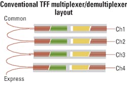
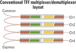
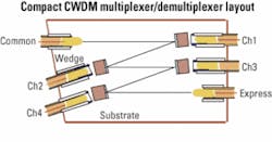
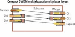
Figure 1 shows a typical current TFF multiplexer/demultiplexer module implementation where three-port TFF devices are first made and then integrated through fiber splicing and routing. The disadvantages are that the overall module insertion loss is compounded each time a device is cascaded due to unnecessary free-space-to-fiber conversion steps, and that the final module dimension has to include the space consumed by fiber routing, which makes a bulky package.In Figure 3, a modified architecture for the CDWDM is presented where several key changes from the Figure 2 system can be noted. First, filters and collimating optics are integrated before this subassembly is integrated again on the substrate level for module formation. Second, the filters’ AOI is arranged to be substantially smaller than in the CCWDM case. These changes enable an accurate wavelength control to about 0.03 nm or equivalently 0.15° of angular tuning and an overall packaging box dimension of 45×25×8 mm.
For DWDM applications, two major factors require the accurate wavelength control of multiplexer/demultiplexer devices. The first is the narrow channel spacing: 1.6 nm for 200 GHz and 0.8 nm for 100 GHz. The second is the coating yield: Without a central AOI tuning mechanism, the central wavelength of coating should be controlled accurately, which is very difficult for DWDM dielectric coatings. Usually, within a coating wafer, the resultant central wavelengths vary due to fluctuations in the thin-film layer thickness. Thus, only a small central area has the right wavelength for a specified DWDM channel. A good tuning method enables the use of a range of wavelengths, thus enlarging the usable area of the filter wafer.For 100 GHz, the central wavelength control accuracy must be within 0.05 nm, which means 0.15° of incidence angle control at a nominal AOI of 1.8°. It is not practical to use the conventional method, i.e., directly rotating a filter by hand, to achieve this target. Additionally, after getting the right wavelength, securing the wavelength throughout the device lifetime is most critical.
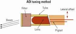
These issues have been successfully solved by the filter-collimator subassembly design. As shown in Figure 4, the filter is bonded to a tube end-face. The other end of the tube is polished to fit the polish angles (8°) of the lens and the dual-fiber pigtail. The distance between two fibers in the pigtail is set to tilt the out beam from the collimator to the specified AOI. To compensate for possible manufacturing errors of fiber distance and coating wavelength, the pigtail can be displaced laterally. After both the central wavelength of the filter and the minimum loss of the collimator have been obtained, the pigtail is secured to the tube. The angle tuning relationship is dθ = dx/f, where dθ, dx, and f denote angle change, lateral offset, and collimator focal length, respectively. For f = 1.93 mm, to meet a 0.02-nm wavelength adjustment, a maximum 2 µm of offset dx is required.
During device building, the in-process control of the center wavelength is set at 0.03 nm. More than 80% of center-wavelength errors of 100 channels fall within 0.02 nm.
As shown in Figure 3, a CDWDM device consists of multiple filter-collimator subassemblies bonded to a common substrate. Wedges are used to fill the gap between collimators and the substrate and are fixed by epoxy. This flexible structure performs excellently despite changes in ambient conditions.
The entire device works in a similar way as a CCWDM. The input multiplexed signals from the common port propagate to channel 1. The filter passband wavelength of this channel passes through; other wavelengths are reflected to channel 2 and are manipulated in the same manner, until all drop channels have been coupled out. Then the remaining signals exit from the express port.
The filter’s AOI is configured so that CDWDM works at a middle range of AOI (about 4.5°) for which the coating performance and optical path lengths are optimally designed. Compared with regular three-port device filters, the central wavelength of a CDWDM subassembly offsets 1.6 nm, i.e., two channel grids for 100 GHz and one channel grid for 200 GHz. Due to the s-polarization and p-polarization splitting, the bandwidth shrinkage is about 0.05 nm, which is within the tolerable range.
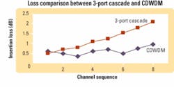
To increase the transmission distance between two optical amplifiers, it is critical to minimize the insertion loss of multiplexer/demultiplexer devices. The root causes of device loss are collimator-to-collimator coupling loss and accumulated filter loss. The worst insertion loss among channels of an n-channel three-port DWDM and CDWDM can be estimated as Σ(ILcollimator)n + Σ(ILfilter,R)n-1 + ILfilter,Tand ILcollimator + Σ(ILfilter,R)n-1 + ILfilter,T, respectively. More specifically, the practical pair collimator loss is around 0.20 dB, filter reflection loss is typically below 0.005 dB to achieve transmission isolation requirements of 30 dB, and filter transmission loss is typically less than 0.25 dB.
By using the formula above, it can be seen that the three-port cascaded-filter approach can offer 1.1- and 1.9-dB worst insertion losses for four-channel and eight-channel modules, respectively. The CDWDM approach, however, can deliver 0.47 and 0.49 dB for the same two cases under the same assumptions, respectively. This loss estimation is based on the assumption that all collimator pairs are perfectly matched (0.20 dB). For practical devices, more coupling loss is seen due to nonperfect matching.Daoyi Wang is senior optical engineer and Yao Li is chief technologist at Alliance Fiber Optic Products, Inc. (Sunnyvale, CA; www.afop.com). Wang can be reached at [email protected].
