by Ryan Latchman and Bharat Tailor
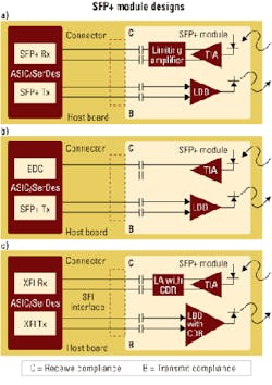
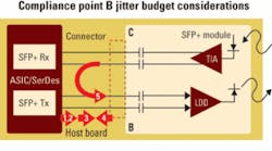
SFP+ is the latest pluggable optical module form factor for use in 10-Gbit/sec Ethernet and 8.5-Gbit/sec Fibre Channel systems. The objectives of this new form factor are to increase density through its smaller footprint and provide a low-cost module to help enable increased adoption. Semiconductor companies and module vendors have begun to offer products for this space that can be used in a number of potential system architectures. This article investigates these architectures as they apply to Fibre Channel and Ethernet and discusses the merits of each in relation to SFP+ objectives. SFP+ designs Figure 1 depicts block diagrams of typical SFP+ module designs targeted for Fibre Channel and Ethernet applications. Two variants of SFP+ are currently being specified. The limiting variant, which closely resembles current SFP modules, includes a laser driver, a TOSA, a ROSA, and a limiting amplifier. The second variant, which is primarily intended for 10-Gbit/sec Ethernet long-reach legacy multimode (LRM) applications, requires a linear optical receive path and is therefore referred to as the linear variant. A third variant that is compliant with SFP+, although not explicitly defined by the standard, is the retimed variant. This variant integrates CDR functionality within the Tx and/or Rx path and resolves signal integrity challenges inherent to many high-speed systems. Current 10-Gbit/sec modules (300-pin, XENÂPAK, XPAK, X2, XFP) guarantee physical layer compliance to standards since the host board design has little or no impact on optical link performance. In contrast, SFP+ modules present relatively new challenges for IC, module, and system designers since standards compliance is determined by the interaction of the system, module, and ICs. The linear variant, where the binary 1/0 decisions are made outside the module, is arguably the most difficult to design with, while the retimed variant is comparatively easy. Transmit direction considerations Linear and limiting SFP+ modules require high-quality ASIC/SerDes transmitters because IEEE and Fibre Channel standards place strict requirements on the optical interface and linear/limiting module types have Tx paths that do not correct for timing jitter. The SFP+ specification has not defined the required jitter performance for the ASIC/SerDes to meet the compliance point B specification. Instead, only the jitter requirement at B is given. This introduces a design challenge for system vendors and host ASIC/SerDes providers to mutually guarantee performance over production (IC to IC variation and PCB build variation) and operating conditions (temperature, voltage, humidity, etc.).The design challenge at compliance point B is heightened by the relatively low amount of permitted jitter at this interface, which must be allocated between the host and the IC. The current SFP+ draft permits a maximum of 0.1 UIpp (or 9.7 psec at 10.3125 Gbits/sec) of data-dependent jitter (DDJ) and 0.055 UIpp (or 5.3 psec at 10.3125 Gbits/sec) of pulsewidth shrinkage (PWS). In many respects, this level of jitter performance is comparable to what is required in SONET/SDH systems, which have a jitter generation requirement of 0.1 UIpp and operate at a physical layer that has not been able to achieve the low cost of Ethernet and Fibre Channel. Guaranteeing this level of jitter will most likely involve statistical analysis and guard-banding. One must also allocate portions of this budget for contributors shown in the modified reference model in Fig. 2. Each of these contributors affects the implementation cost for non-retimed SFP+.
Since deterministic jitter is not a scalar quantity (i.e., it has an associated phase), the combination of the aforementioned contributors plus an optical module, when measured in the lab, may be less than the sum of the individual jitter contributors. In this case, deterministic jitter components are cancelling each other out. This cancellation, however, is not controlled or monitored in typical IC/system production environments and is therefore difficult to rely on. Also, since SFP+ modules are pluggable, field installation could lead to uncertain performance. An arithmetic summing of peak-to-peak values should be considered. Module vendors must also consider the potential types of jitter that can be presented to the module and ensure a compliant output from the module. In an effort to address the jitter contributors mentioned, some silicon vendors have designed host repeater ICs that are intended to minimize the burden on 10G serial ASICs. These ICs assist with SFI channel concerns through relative layout flexibility compared to ASICs, but do not solve them; standard compliance is still dependent on the interaction between the host, the SFI repeater, and the optical module. The SFI channel between the repeater and the laser driver will invariably introduce more jitter than if the repeater were right beside the laser driver inside the optical module.
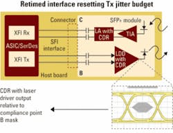
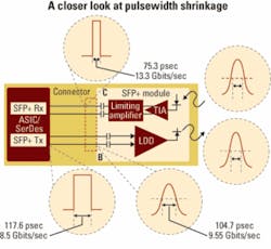
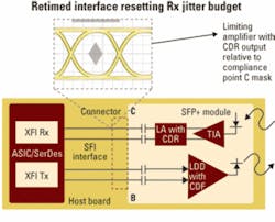
These host and module design issues can be greatly simplified by putting a repeater (or CDR) in the transmit direction within the SFP+ module. This CDR would reset the jitter budget within the module, eliminating the need for an IC between the ASIC and the module in the Tx direction, and greatly relax the required jitter performance from the ASIC. This corresponds to the retimed architecture depicted in Fig. 3. The CDR functionality does increase power consumption marginally within the SFP+ module, but modules can still meet the less than 1-W Power Level I requirement. The CDR provides a well proven host-module interface that ensures standards compliance by resetting the jitter budget within the optical module. When a CDR is present in the module, one can expect the equivalent performance and robustness from the SFP+ system as an X2/XFP system, which in turn lowers development, test, and manufacturing costs. SFP+ receive direction In the receive direction, SFP+ retimed, limiting, and linear interfaces differ significantly. In the limiting interface, a binary 1/0 decision is made in amplitude but not in time. This results in squaring of the waveform, but jitter from the signal after O-to-E conversion is still present at the SFP+ connector. This is reflected in the limiting output jitter specification for Fibre Channel and Ethernet (draft values 0.71 UIpp and 0.7 UIpp, Ârespectively). In addition to the large jitter permitted at the output of the limiting interface, a special type of jitter has been defined: PWS. This special type of jitter can be particularly challenging since narrower pulses get attenuated to a greater extent when transmitted over lossy media and therefore require much higher bandwidth circuitry to recover and properly interpret received data.
The linear module type shifts the majority of the standard compliance onto the host board since 1/0 decisions are not made within the module at all. In fact, this module class requires very good linearity in the receive path over all operating conditions. Even with optimal linearity, additional challenges arise due to crosstalk and SFI/module channel loss with reflections. This makes an already challenging LRM specification even more difficult to meet by placing the EDC chip on the host board and not within the module. Linear modules also typically have lower gain than limiting modules, making output amplitudes smaller and potentially more difficult for hosts to recover.
Properly designed EDC chips are, however, able to compensate for LRM stressors. Depending on margin, they may be able to be used for receive direction link compliance, although EDC can increase the power consumption and the cost of a serial PHY by a significant factor.
Architecture summary
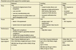
Each of the three architectures discussed in this article has an associated cost, power, and performance. The table summarizes the potential cost for each module type along with potential link support.
System, module, and IC designers have provided the high-speed communications market with a number of implementation options for SFP+. Depending on application performance and cost requirements, an implementation can benefit from some or all of these options. Having a solid physical layer design ensures standards compliance over operating conditions and production, and can provide system designers the flexibility for design changes to line cards without having to worry about the impact to the physical layer compliance or pluggable module interoperability.
Ryan Latchmanis a senior product definition specialist andBharat Tailoris a director of marketing in the Analog and Mixed Signal Products Division at Gennum (www.gennum.com).
For more optical equipment design information, visit the Optical Equipment Design Center
