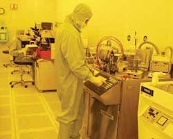
So it only makes sense to find someone else to help fill your unused fab capacity, particularly if that someone will pay you to do it. With the depression in the optical communications market, most of the companies interested in accessing unused wafer capabilities fell outside of the telecommunications arena. Avanex (www.avanex.com), for example, found interest from companies in the military and biomedical fields. This interest not only helped Avanex offset the cost of its fabrication assets but proved to have strategic advantages as well.
“Companies like Avanex went through really rough times over the last 2 or 3 years. We always felt that there were opportunities outside of our core market that we wanted to continue to monitor and be involved in, but where we basically couldn’t afford to invest in a business development team or a pure R&D effort,” explains Yves Le Maitre, vice president and general manager of Avanex’s Components Business Unit. “At a time when the optoelectronics industry had to go through so much restructuring and cost cutting, to have the ability to use these kinds of partnerships on real programs with real customers, to continue to develop new technologies and new processes, was actually something that we found very interesting.”
CyOptics (www.cyoptics.com), which acquired advanced wafer fabrication and processing capabilities in Pennsylvania through its acquisition of what used to be Lucent’s Microelectronics Group from TriQuint Semiconductor, saw interest from academia, companies working on government projects, and commercial industry. According to chief executive officer Ed Goringrato, the return of relative prosperity to the optical communications industry has been reflected in his foundry business.
“From a volume perspective, it’s the commercial customers,” Goringrato says of his largest market. “The academia is running a few wafers; it’s probably not going to go into volume production anytime soon.”
Goringrato estimates that most of CyOptics’ foundry services clients are in the optical communications space. “It’s mainly the folks who are fabless. They’re looking for a fab house. But quite honestly, we’re also starting to interact with folks that have fabs themselves. They’ve just realized that they can’t do everything themselves; they don’t have an in-house capability. And they continuously look at that make-versus-buy decision.”
Le Maitre says that approximately 50% of Avanex’s foundry business is in communications. However, the company is very selective about what companies it will engage, staying away from current or potential competitors in its core markets of optical components and subsystems for metro, long-haul, and submarine markets. “You want to make sure that the projects that the customers have fit with our strategies,” he explains, “So it’s something that hopefully will help us improve our own processes in telecom. It’s something that will need to go to an industrialization phase, so it means it’s a project-obviously you don’t know when you start, but there is an opportunity that is fairly sizeable in the long run that can generate production of particular wafers with a need to have an infrastructure behind it.”
Right now, Le Maitre sees such an opportunity in triplexers, particularly people looking for Fabry-Perot laser chips. Interestingly, CyOptics reports significant interest from companies using planar lightwave circuit technology for FTTH transceivers as well.
The current generation of fabless companies has a wide variety of requirements-and both Avanex and CyOptics provide an extensive menu of services. According to Bryan Segner, vice president of wafer fab engineering and operations at CyOptics, the company’s foundry services can be roughly divided into three main stages. The first is epitaxial growth and characterization, where they would grow atomic layers of material to perform different functions within the device. Second is wafer fabrication, where CyOptics will perform process steps such as metallization for contact layers, etching, etc. The final stage would be chip fabrication and testing, where they would take the fully processed wafer, dice it up into chips, and test. CyOptics works primarily in indium phosphide (InP), although it can handle some gallium arsenide (GaAs) processes as well. The company also will place finished chips on submounts.
Goringrato adds that CyOptics has a “tool box” of designs based on work the company has done with some of its existing or past products. This includes Fabry-Perot, distributed feedback, and externally modulated lasers; PIN and avalanche photodiode receivers; arrayed waveguide gratings; semiconductor optical amplifiers; and others.
Avanex also offers a complete set of wafer fabrication, processing, and test services, as well as the benefit of expertise gained through its own design activities. Most of Avanex’s foundry services are offered via its InP and GaAs capabilities in Nozay, France; a facility in Italy has been used to provide lithium niobate services for gyroscope components, Le Maitre says.
The sources at both companies say that they have customers who use a complete set of services and some that only use one or two elements. They say that customers generally begin by asking what kinds of substrates do the foundry services offer and then move to what kinds of processes or added value beyond the substrate are available and desired. Le Maitre says that customers then frequently ask very specific questions to make their final decisions. “It boils down in many cases to the type of machines and reactors that you have in your fab,” he adds.
How many places potential customers can go depends upon what they want. There are about 50 fab houses from which customers can choose, Le Maitre estimates. However, if the customer is looking for someone with a background in telecommunications, the options shrink to about 10, if you don’t include universities (which typically offer limited fab services) and specialty niche players. Le Maitre lists Mitsubishi, Hitachi, and Fujitsu in Japan and companies such as Finisar and Bookham in the West as examples.
Neither Avanex nor CyOptics expects the revenue from foundry services to rival that of their component businesses. In most cases, it’s difficult to know how much of an opportunity there is. “A lot of the opportunities that you get a lot of times are forward looking; they come to you with the tough stuff, sometimes,” explains Goringrato. “It’s something that’s probably going to get to market on a volume basis in…it could be 18 months.”
Still, the trend toward fabless business models doesn’t show signs of slowing, which means that continued health in the overall optical communications market should translate into continued foundry service business. Referring to the more than 10,000 sq. ft. of Class 1000 cleanroom facilities at Avanex’s disposal, Le Maitre comments, “That’s an investment we made in the glory days of 1999/2000. There are very few people who could afford that today.”Last November, the Optoelectronics Industry Development Association (OIDA), in conjunction with Defense Advanced Research Projects Agency’s Photonic Technology Access Project (PTAP), held a workshop to explore whether a foundry model similar to that enjoyed by the IC arena would make sense in optoelectronics-and, if so, what such a model would look like. (See “OIDA Explores Optical Foundry Model,” Lightwave, January 2006, page 1.) Not surprisingly, given the many ways that a laser can be designed and manufactured, the workshop provided as many questions as answers.
Undaunted, OIDA has continued to work toward establishing an optoelectronics foundry model. Marko Slusarczuk, director of government programs at OIDA and the organization ’s main liaison with PTAP, says the effort is currently in a research phase that involves determining what kinds of processes and capabilities are available, who is providing them, and what kind of potential customers would most likely use them initially. The idea, says Slusarczuk, is to recruit entities interested in pursuing a foundry model, then help them use such a model to create useful devices.
Slusarczuk says that defense and academia would likely make the best initial clients for such a model, the former because of the interest in developing cutting-edge technologies within the United States, the latter because, as Slusarczuk put it, “no one will go out of business if the process doesn’t work.” That process would involve what he called a “virtual foundry” because of the lack of interest in building a new foundry facility when so many existing ones are underused.
The current investigative phase should continue for several more months, Slusarczuk predicts, before implementation begins. A sponsor, likely from the government side, would also be necessary.

